 Lapsed, fee not paid8 drawings
Cameras, Displays & Optics · US 8,599,123 B2
Drive circuit and liquid crystal display using the same
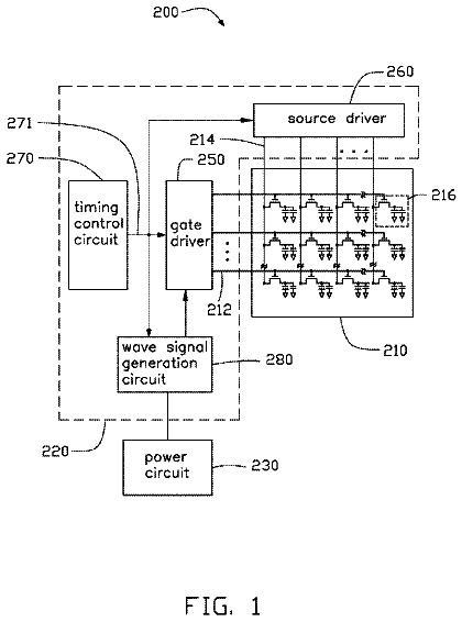
A liquid crystal display includes a liquid crystal panel, a drive circuit, and a power circuit.
US 8,599,191 B2 · Assignee: Ignis Innovation Inc. · Inventors: Chaja; Gholamreza et al.
Sheet 1 of 13 from the published document. All sheets in the USPTO PDF
A system to improve the extraction of transistor and OLED parameters in an AMOLED display includes a pixel circuit having an organic light emitting device, a drive device to provide a programmable drive current to the light emitting device, a programming input to provide the programming signal, and a storage device to store the programming signal. A charge-pump amplifier has a current input and a voltage output. The charge-pump amplifier includes an operational amplifier in negative feedback configuration. The feedback is provided by a capacitor connected between the output and the inverting input of the operational amplifier. A common-mode voltage source drives the non-inverting input of the operational amplifier. An electronic switch is coupled across the capacitor to reset the capacitor. A switch module including the input is coupled to the output of the pixel circuit and an output is coupled to the input of the charge-pump amplifier.
Currently, active matrix organic light emitting device ("AMOLED") displays are being introduced. The advantages of such displays include lower power consumption, manufacturing flexibility and faster refresh rate over conventional liquid crystal displays. In contrast to conventional liquid crystal displays, there is no backlighting in an AMOLED display, and thus each pixel consists of different colored OLEDs emitting light independently. The OLEDs emit light based on current supplied through a drive transistor controlled by a programming voltage. The power consumed in each pixel has a relation with the magnitude of the generated light in that pixel. The quality of output in an OLED based pixel is affected by the properties of the drive transistor, which is typically fabricated from materials including but not limited to amorphous silicon, polysilicon, or metal oxide, as well as the OLED i
8 of 13 drawing sheets so far from the published document, cropped to the drawing. Every sheet is in the USPTO PDF.
What the patent claimed, word for word. All of it is now free to use.
The present invention generally relates to active matrix organic light emitting device (AMOLED) displays, and particularly extracting threshold and mobility factors from the pixel drivers for such displays.
Currently, active matrix organic light emitting device ("AMOLED") displays are being introduced. The advantages of such displays include lower power consumption, manufacturing flexibility and faster refresh rate over conventional liquid crystal displays. In contrast to conventional liquid crystal displays, there is no backlighting in an AMOLED display, and thus each pixel consists of different colored OLEDs emitting light independently. The OLEDs emit light based on current supplied through a drive transistor controlled by a programming voltage. The power consumed in each pixel has a relation with the magnitude of the generated light in that pixel.
The quality of output in an OLED based pixel is affected by the properties of the drive transistor, which is typically fabricated from materials including but not limited to amorphous silicon, polysilicon, or metal oxide, as well as the OLED itself. In particular, threshold voltage and mobility of the drive transistor tend to change as the pixel ages. In order to maintain image quality, changes in these parameters must be compensated for by adjusting the programming voltage. In order to do so, such parameters must be extracted from the driver circuit. The addition of components to extract such parameters in a simple driver circuit requires more space on a display substrate for the drive circuitry and thereby reduces the amount of aperture or area of light emission from the OLED.
When biased in saturation, the I-V characteristic of a thin film drive transistor depends on mobility and threshold voltage which are a function of the materials used to fabricate the transistor. Thus different thin film transistor devices implemented across the display panel may demonstrate non-uniform behavior due to aging and process variations in mobility and threshold voltage. Accordingly, for a constant voltage, each device may have a different drain current. An extreme example may be where one device could have low threshold-voltage and low mobility compared to a second device with high threshold-voltage and high mobility.
Thus with very few electronic components available to maintain a desired aperture, extraction of non-uniformity parameters (i.e. threshold voltage, V.sub.th, and mobility, .mu.) of the drive TFT and the OLED becomes challenging. It would be desirable to extract such parameters in a driver circuit for an OLED pixel with as few components as possible to maximize pixel aperture.
One example disclosed is a data extraction system for an organic light emitting device (OLED) based display. The system includes a pixel circuit including an organic light emitting device, a drive device to provide a programmable drive current to the light emitting device, a programming input to provide a programming signal, and a storage device to store the programming signal. A charge-pump amplifier has a current input and a voltage output. The charge-pump amplifier includes an operational amplifier in negative feedback configuration. The feedback is provided by a capacitor connected between the output and the inverting input of the operational amplifier. A common-mode voltage source drives the non-inverting input of the operational amplifier. An electronic switch is coupled across the capacitor to reset the capacitor. A switch module including the input is coupled to the output of the pixel circuit and an output is coupled to the input of the charge-pump amplifier. The switch module includes a plurality of electronic switches that may be controlled by external control signals to steer current in and out of the pixel circuit, provide a discharge path between the pixel circuit and the charge-pump amplifier and isolate the charge-pump amplifier from the pixel circuit. A controller is coupled to the pixel circuit, charge-pump amplifier and the switch module. The controller controls input signals to the pixel circuit, charge-pump amplifier and switch module in a predetermined sequence to produce an output voltage value which is a function of a parameter of the pixel circuit. The sequence includes providing a program voltage to the programming input to either pre-charge an internal capacitance of the pixel circuit to a charge level and transfer the charge to the charge-pump amplifier via the switch module to generate the output voltage value or provide a current from the pixel circuit to the charge-pump amplifier via the switch module to produce the output voltage value by integration over a certain period of time.
Another example is a method of extracting a circuit parameter from a pixel circuit including an organic light emitting device, a drive device to provide a programmable drive current to the light emitting device, a programming input, and a storage device to store a programming signal. A predetermined program voltage is provided to the programming voltage input. A capacitance of the pixel circuit is charged to a charge level or a current from the pixel circuit. The pixel circuit is coupled to a charge-pump amplifier. The charge-pump amplifier is isolated from the pixel circuit to provide a voltage output either proportional to the charge level or to integrate the current from the pixel circuit. The voltage output of the charge-pump amplifier is read. At least one pixel circuit parameter is determined from the voltage output of the charge-pump amplifier.
Another example is a data extraction system for an organic light emitting device (OLED) based display. The system includes a pixel circuit having a drive transistor, an organic light emitting device, and a programming input coupled to the gate of the drive transistor. The drive transistor has a source or a drain coupled to the OLED. A charge-pump amplifier has an input and an integrated voltage output. A switch module includes an input coupled to the output of the pixel circuit and an output coupled to the input of the charge-pump amplifier. The switch module includes switches to steer current in and out of the pixel circuit, provide a discharge path between the pixel circuit and the charge-pump amplifier and isolate the charge-pump amplifier from the pixel circuit. A controller is coupled to the pixel circuit, charge-pump amplifier and the switch module. The controller controls voltage inputs to the pixel circuit, charge-pump amplifier and switch module in a predetermined sequence to produce an output voltage value which is a function of a parameter of the pixel circuit. The sequence including providing a program voltage to the programming input to either pre-charge a capacitance of the pixel circuit to a charge level, transfer the charge to the charge-pump amplifier via the switch module to generate the output voltage value or provide a current from the pixel circuit to the charge-pump amplifier via the switch module to produce the output voltage value by integration.
The foregoing and additional aspects and embodiments of the present invention will be apparent to those of ordinary skill in the art in view of the detailed description of various embodiments and/or aspects, which is made with reference to the drawings, a brief description of which is provided next.
The foregoing and other advantages of the invention will become apparent upon reading the following detailed description and upon reference to the drawings.
FIG. 1 is a block diagram of an AMOLED display with compensation control;
FIG. 2 is a circuit diagram of a data extraction circuit for a two-transistor pixel in the AMOLED display in FIG. 1;
FIG. 3A is a signal timing diagram of the signals to the data extraction circuit to extract the threshold voltage and mobility of an n-type drive transistor in FIG. 2;
FIG. 3B is a signal timing diagram of the signals to the data extraction circuit to extract the characteristic voltage of the OLED in FIG. 2 with an n-type drive transistor;
FIG. 3C is a signal timing diagram of the signals to the data extraction circuit for a direct read to extract the threshold voltage of an n-type drive transistor in FIG. 2;
FIG. 4A is a signal timing diagram of the signals to the data extraction circuit to extract the threshold voltage and mobility of a p-type drive transistor in FIG. 2;
FIG. 4B is a signal timing diagram of the signals to the data extraction circuit to extract the characteristic voltage of the OLED in FIG. 2 with a p-type drive transistor;
FIG. 4C is a signal timing diagram of the signals to the data extraction circuit for a direct read to extract the threshold voltage of a p-type drive transistor in FIG. 2;
FIG. 4D is a signal timing diagram of the signals to the data extraction circuit for a direct read of the OLED turn-on voltage using either an n-type or p-type drive transistor in FIG. 2.
FIG. 5 is a circuit diagram of a data extraction circuit for a three-transistor drive circuit for a pixel in the AMOLED display in FIG. 1 for extraction of parameters;
FIG. 6A is a signal timing diagram of the signals to the data extraction circuit to extract the threshold voltage and mobility of the drive transistor in FIG. 5;
FIG. 6B is a signal timing diagram of the signals to the data extraction circuit to extract the characteristic voltage of the OLED in FIG. 5;
FIG. 6C is a signal timing diagram the signals to the data extraction circuit for a direct read to extract the threshold voltage of the drive transistor in FIG. 5;
FIG. 6D is a signal timing diagram of the signals to the data extraction circuit for a direct read to extract the characteristic voltage of the OLED in FIG. 5;
FIG. 7 is a flow diagram of the extraction cycle to readout the characteristics of the drive transistor and the OLED of a pixel circuit in an AMOLED display;
FIG. 8 is a flow diagram of different parameter extraction cycles and final applications; and
FIG. 9 is a block diagram and chart of the components of a data extraction system.
FIG. 10 is a signal timing diagram of the signals to the data extraction circuit to extract the threshold voltage and mobility of the drive transistor in a modified version of the circuit in FIG. 5; and
FIG. 11 is a signal timing diagram of the signals to the data extraction circuit to extract the characteristic voltage of the OLED in a modified version of the circuit in FIG. 5;
While the invention is susceptible to various modifications and alternative forms, specific embodiments have been shown by way of example in the drawings and will be described in detail herein. It should be understood, however, that the invention is not intended to be limited to the particular forms disclosed. Rather, the invention is to cover all modifications, equivalents, and alternatives falling within the spirit and scope of the invention as defined by the appended claims.
FIG. 1 is an electronic display system 100 having an active matrix area or pixel array 102 in which an n.times.m array of pixels 104 are arranged in a row and column configuration. For ease of illustration, only two rows and two columns are shown. External to the active matrix area of the pixel array 102 is a peripheral area 106 where peripheral circuitry for driving and controlling the pixel array 102 are disposed. The peripheral circuitry includes an address or gate driver circuit 108, a data or source driver circuit 110, a controller 112, and an optional supply voltage (e.g., Vdd) driver 114. The controller 112 controls the gate, source, and supply voltage drivers 108, 110, 114. The gate driver 108, under control of the controller 112, operates on address or select lines SEL[i], SEL[i+1], and so forth, one for each row of pixels 104 in the pixel array 102. In pixel sharing configurations described below, the gate or address driver circuit 108 can also optionally operate on global select lines GSEL[j] and optionally /GSEL[j], which operate on multiple rows of pixels 104 in the pixel array 102, such as every two rows of pixels 104. The source driver circuit 110, under control of the controller 112, operates on voltage data lines Vdata[k], Vdata[k+1], and so forth, one for each column of pixels 104 in the pixel array 102. The voltage data lines carry voltage programming information to each pixel 104 indicative of the brightness of each light emitting device in the pixel 104. A storage element, such as a capacitor, in each pixel 104 stores the voltage programming information until an emission or driving cycle turns on the light emitting device. The optional supply voltage driver 114, under control of the controller 112, controls a supply voltage (EL_Vdd) line, one for each row or column of pixels 104 in the pixel array 102.
The display system 100 further includes a current supply and readout circuit 120, which reads output data from data output lines, VD [k], VD [k+1], and so forth, one for each column of pixels 104 in the pixel array 102.
As is known, each pixel 104 in the display system 100 needs to be programmed with information indicating the brightness of the light emitting device in the pixel 104. A frame defines the time period that includes: (i) a programming cycle or phase during which each and every pixel in the display system 100 is programmed with a programming voltage indicative of a brightness; and (ii) a driving or emission cycle or phase during which each light emitting device in each pixel is turned on to emit light at a brightness commensurate with the programming voltage stored in a storage element. A frame is thus one of many still images that compose a complete moving picture displayed on the display system 100. There are at least schemes for programming and driving the pixels: row-by-row, or frame-by-frame. In row-by-row programming, a row of pixels is programmed and then driven before the next row of pixels is programmed and driven. In frame-by-frame programming, all rows of pixels in the display system 100 are programmed first, and all rows of pixels are driven at once. Either scheme can employ a brief vertical blanking time at the beginning or end of each frame during which the pixels are neither programmed nor driven.
The components located outside of the pixel array 102 may be disposed in a peripheral area 106 around the pixel array 102 on the same physical substrate on which the pixel array 102 is disposed. These components include the gate driver 108, the source driver 110, the optional supply voltage driver 114, and a current supply and readout circuit 120. Alternately, some of the components in the peripheral area 106 may be disposed on the same substrate as the pixel array 102 while other components are disposed on a different substrate, or all of the components in the peripheral area can be disposed on a substrate different from the substrate on which the pixel array 102 is disposed. Together, the gate driver 108, the source driver 110, and the supply voltage driver 114 make up a display driver circuit. The display driver circuit in some configurations can include the gate driver 108 and the source driver 110 but not the supply voltage control 114.
When biased in saturation, the first order I-V characteristic of a metal oxide semiconductor (MOS) transistor (a thin film transistor in this case of interest) is modeled as:
.times..mu..times..times..times..times. ##EQU00001## where I.sub.D is the drain current and V.sub.GS is the voltage difference applied between gate and source terminals of the transistor. The thin film transistor devices implemented across the display system 100 demonstrate non-uniform behavior due to aging and process variations in mobility (.mu.) and threshold voltage (V.sub.th). Accordingly, for a constant voltage difference applied between gate and source, V.sub.GS, each transistor on the pixel matrix 102 may have a different drain current based on a non-deterministic mobility and threshold voltage: I.sub.D(i,j)=f(.mu..sub.i,j, V.sub.th i,j) where i and j are the coordinates (row and column) of a pixel in an n.times.m array of pixels such as the array of pixels 102 in FIG. 1.
FIG. 2 shows a data extraction system 200 including a two-transistor (2 T) driver circuit 202 and a readout circuit 204. The supply voltage control 114 is optional in a display system with 2 T pixel circuit 104. The readout circuit 204 is part of the current supply and readout circuit 120 and gathers data from a column of pixels 104 as shown in FIG. 1. The readout circuit 204 includes a charge pump circuit 206 and a switch-box circuit 208. A voltage source 210 provides the supply voltage to the driver circuit 202 through the switch-box circuit 208. The charge-pump and switch-box circuits 206 and 208 are implemented on the top or bottom side of the array 102 such as in the voltage drive 114 and the current supply and readout circuit 120 in FIG. 1. This is achieved by either direct fabrication on the same substrate as the pixel array 102 or by bonding a microchip on the substrate or a flex as a hybrid solution.
The driver circuit 202 includes a drive transistor 220, an organic light emitting device 222, a drain storage capacitor 224, a source storage capacitor 226, and a select transistor 228. A supply line 212 provides the supply voltage and also a monitor path (for the readout circuit 204) to a column of driver circuits such as the driver circuit 202. A select line input 230 is coupled to the gate of the select transistor 228. A programming data input 232 is coupled to the gate of the drive transistor 220 through the select transistor 228. The drain of the drive transistor 220 is coupled to the supply voltage line 212 and the source of the drive transistor 220 is coupled to the OLED 222. The select transistor 228 controls the coupling of the programming input 230 to the gate of the drive transistor 220. The source storage capacitor 226 is coupled between the gate and the source of the drive transistor 220. The drain storage capacitor 224 is coupled between the gate and the drain of the drive transistor 220. The OLED 222 has a parasitic capacitance that is modeled as a capacitor 240. The supply voltage line 212 also has a parasitic capacitance that is modeled as a capacitor 242. The drive transistor 220 in this example is a thin film transistor that is fabricated from amorphous silicon. Of course other materials such as polysilicon or metal oxide may be used. A node 244 is the circuit node where the source of the drive transistor 220 and the anode of the OLED 222 are coupled together. In this example, the drive transistor 220 is an n-type transistor. The system 200 may be used with a p-type drive transistor in place of the n-type drive transistor 220 as will be explained below.
The readout circuit 204 includes the charge-pump circuit 206 and the switch-box circuit 208. The charge-pump circuit 206 includes an amplifier 250 having a positive and negative input. The negative input of the amplifier 250 is coupled to a capacitor 252 (C.sub.int) in parallel with a switch 254 in a negative feedback loop to an output 256 of the amplifier 250. The switch 254 (S4) is utilized to discharge the capacitor 252 C.sub.int during the pre-charge phase. The positive input of the amplifier 250 is coupled to a common mode voltage input 258 (VCM). The output 256 of the amplifier 250 is indicative of various extracted parameters of the drive transistor 220 and OLED 222 as will be explained below.
The switch-box circuit 208 includes several switches 260, 262 and 264 (S1, S2 and S3) to steer current to and from the pixel driver circuit 202. The switch 260 (S1) is used during the reset phase to provide a discharge path to ground. The switch 262 (S2) provides the supply connection during normal operation of the pixel 104 and also during the integration phase of readout. The switch 264 (S3) is used to isolate the charge-pump circuit 206 from the supply line voltage 212 (VD).
The general readout concept for the two transistor pixel driver circuit 202 for each of the pixels 104, as shown in FIG. 2, comes from the fact that the charge stored on the parasitic capacitance represented by the capacitor 240 across the OLED 222 has useful information of the threshold voltage and mobility of the drive transistor 220 and the turn-on voltage of the OLED 222. The extraction of such parameters may be used for various applications. For example, such parameters may be used to modify the programming data for the pixels 104 to compensate for pixel variations and maintain image quality. Such parameters may also be used to pre-age the pixel array 102. The parameters may also be used to evaluate the process yield for the fabrication of the pixel array 102.
Assuming that the capacitor 240 (C.sub.OLED) is initially discharged, it takes some time for the capacitor 240 (C.sub.OLED) to charge up to a voltage level that turns the drive transistor 220 off. This voltage level is a function of the threshold voltage of the drive transistor 220. The voltage applied to the programming data input 232 (V.sub.Data) must be low enough such that the settled voltage of the OLED 222 (V.sub.OLED) is less than the turn-on threshold voltage of the OLED 222 itself. In this condition, V.sub.Data-V.sub.OLED is a linear function of the threshold voltage (V.sub.th) of the drive transistor 220. In order to extract the mobility of a thin film transistor device such as the drive transistor 220, the transient settling of such devices, which is a function of both the threshold voltage and mobility, is considered. Assuming that the threshold voltage deviation among the TFT devices such as the drive transistor 220 is compensated, the voltage of the node 244 sampled at a constant interval after the beginning of integration is a function of mobility only of the TFT device such as the drive transistor 220 of interest.
FIG. 3A-3C are signal timing diagrams of the control signals applied to the components in FIG. 2 to extract parameters such as voltage threshold and mobility from the drive transistor 220 and the turn on voltage of the OLED 222 in the drive circuit 200 assuming the drive transistor 220 is an n-type transistor. Such control signals could be applied by the controller 112 to the source driver 110, the gate driver 108 and the current supply and readout circuit 120 in FIG. 1. FIG. 3A is a timing diagram showing the signals applied to the extraction circuit 200 to extract the threshold voltage and mobility from the drive transistor 220. FIG. 3A includes a signal 302 for the select input 230 in FIG. 2, a signal 304 (.phi..sub.1) to the switch 260, a signal 306 (.phi..sub.2) for the switch 262, a signal 308 (.phi..sub.3) for the switch 264, a signal 310 (.phi..sub.4) for the switch 254, a programming voltage signal 312 for the programming data input 232 in FIG. 2, a voltage 314 of the node 244 in FIG. 2 and an output voltage signal 316 for the output 256 of the amplifier 250 in FIG. 2.
FIG. 3A shows the four phases of the readout process, a reset phase 320, an integration phase 322, a pre-charge phase 324 and a read phase 326. The process starts by activating a high select signal 302 to the select input 230. The select signal 302 will be kept high throughout the readout process as shown in FIG. 3A.
During the reset phase 320, the input signal 304 (.phi..sub.1) to the switch 260 is set high in order to provide a discharge path to ground. The signals 306, 308 and 310 (.phi..sub.2, .phi..sub.3, .phi.4) to the switches 262, 264 and 250 are kept low in this phase. A high enough voltage level (V.sub.RST.sub.--.sub.TFT) is applied to the programming data input 232 (V.sub.Data) to maximize the current flow through the drive transistor 220. Consequently, the voltage at the node 244 in FIG. 2 is discharged to ground to get ready for the next cycle.
During the integration phase 322, the signal 304 (.phi..sub.2) to the switch 262 stays high which provides a charging path from the voltage source 210 through the switch 262. The signals 304, 308 and 310 (.phi..sub.1, .phi..sub.3, .phi..sub.4) to the switches 260, 264 and 250 are kept low in this phase. The programming voltage input 232 (V.sub.Data) is set to a voltage level (V.sub.INT.sub.--.sub.TFT) such that once the capacitor 240 (C.sub.oled) is fully charged, the voltage at the node 244 is less than the turn-on voltage of the OLED 222. This condition will minimize any interference from the OLED 222 during the reading of the drive transistor 220. Right before the end of integration time, the signal 312 to the programming voltage input 232 (V.sub.Data) is lowered to V.sub.OFF in order to isolate the charge on the capacitor 240 (C.sub.oled) from the rest of the circuit.
When the integration time is long enough, the charge stored on capacitor 240 (C.sub.oled) will be a function of the threshold voltage of the drive transistor 220. For a shortened integration time, the voltage at the node 244 will experience an incomplete settling and the stored charge on the capacitor 240 (C.sub.oled) will be a function of both the threshold voltage and mobility of the drive transistor 220. Accordingly, it is feasible to extract both parameters by taking two separate readings with short and long integration phases.
During the pre-charge phase 324, the signals 304 and 306 (.phi..sub.1, .phi..sub.2) to switches 260 and 262 are set low. Once the input signal 310 (.phi..sub.4) to the switch 254 is set high, the amplifier 250 is set in a unity feedback configuration. In order to protect the output stage of the amplifier 250 against short-circuit current from the supply voltage 210, the signal 308 (.phi..sub.3) to the switch 264 goes high when the signal 306 (.phi..sub.2) to the switch 262 is set low. When the switch 264 is closed, the parasitic capacitance 242 of the supply line is precharged to the common mode voltage, VCM. The common mode voltage, VCM, is a voltage level which must be lower than the ON voltage of the OLED 222. Right before the end of pre-charge phase, the signal 310 (.phi..sub.4) to the switch 254 is set low to prepare the charge pump amplifier 250 for the read cycle.
During the read phase 336, the signals 304, 306 and 310 (.phi..sub.1, .phi..sub.2, .phi..sub.4) to the switches 260, 262 and 254 are set low. The signal 308 (.phi..sub.3) to the switch 264 is kept high to provide a charge transfer path from the drive circuit 202 to the charge-pump amplifier 250. A high enough voltage 312 (V.sub.RD.sub.--.sub.TFT) is applied to the programming voltage input 232 (V.sub.Data) to minimize the channel resistance of the drive transistor 220. If the integration cycle is long enough, the accumulated charge on the capacitor 252 (C.sub.int) is not a function of integration time. Accordingly, the output voltage of the charge-pump amplifier 250 in this case is equal to:
.times. ##EQU00002## For a shortened integration time, the accumulated charge on the capacitor 252 (C.sub.int) is given by:
.intg..times..function..mu.d ##EQU00003## Consequently, the output voltage 256 of the charge-pump amplifier 250 at the end of read cycle equals:
.intg..times..function..mu.d ##EQU00004## Hence, the threshold voltage and the mobility of the drive transistor 220 may be extracted by reading the output voltage 256 of the amplifier 250 in the middle and at the end of the read phase 326.
FIG. 3B is a timing diagram for the reading process of the threshold turn-on voltage parameter of the OLED 222 in FIG. 2. The reading process of the OLED 222 also includes four phases, a reset phase 340, an integration phase 342, a pre-charge phase 344 and a read phase 346. Just like the reading process for the drive transistor 220 in FIG. 3A, the reading process for OLED starts by activating the select input 230 with a high select signal 302. The timing of the signals 304, 306, 308, and 310 (.phi..sub.1, .phi..sub.2, .phi..sub.3, .phi..sub.4) to the switches 260, 262, 264 and 254 is the same as the read process for the drive transistor 220 in FIG. 3A. A programming signal 332 for the programming input 232, a signal 334 for the node 244 and an output signal 336 for the output of the amplifier 250 are different from the signals in FIG. 3A.
During the reset phase 340, a high enough voltage level 332 (V.sub.RST.sub.--.sub.OLED) is applied to the programming data input 232 (V.sub.Data) to maximize the current flow through the drive transistor 220. Consequently, the voltage at the node 244 in FIG. 2 is discharged to ground through the switch 260 to get ready for the next cycle.
During the integration phase 342, the signal 306 (.phi..sub.2) to the switch 262 stays high which provides a charging path from the voltage source 210 through the switch 262. The programming voltage input 232 (V.sub.Data) is set to a voltage level 332 (V.sub.INT.sub.--.sub.OLED) such that once the capacitor 240 (C.sub.oled) is fully charged, the voltage at the node 244 is greater than the turn-on voltage of the OLED 222. In this case, by the end of the integration phase 342, the drive transistor 220 is driving a constant current through the OLED 222.
During the pre-charge phase 344, the drive transistor 220 is turned off by the signal 332 to the programming input 232. The capacitor 240 (C.sub.oled) is allowed to discharge until it reaches the turn-on voltage of OLED 222 by the end of the pre-charge phase 344.
During the read phase 346, a high enough voltage 332 (V.sub.RD.sub.--.sub.OLED) is applied to the programming voltage input 232 (V.sub.Data) to minimize the channel resistance of the drive transistor 220. If the pre-charge phase is long enough, the settled voltage across the capacitor 252 (C.sub.int) will not be a function of pre-charge time. Consequently, the output voltage 256 of the charge-pump amplifier 250 at the end of the read phase is given by:
##EQU00005## The signal 308 (.phi..sub.3) to the switch 264 is kept high to provide a charge transfer path from the drive circuit 202 to the charge-pump amplifier 250. Thus the output voltage signal 336 may be used to determine the turn-on voltage of the OLED 220.
FIG. 3C is a timing diagram for the direct reading of the drive transistor 220 using the extraction circuit 200 in FIG. 2. The direct reading process has a reset phase 350, a pre-charge phase 352 and an integrate/read phase 354. The readout process is initiated by activating the select input 230 in FIG. 2. The select signal 302 to the select input 230 is kept high throughout the readout process as shown in FIG. 3C. The signals 364 and 366 (.phi..sub.1, .phi..sub.2) for the switches 260 and 262 are inactive in this readout process.
During the reset phase 350, the signals 368 and 370 (.phi..sub.3, .phi..sub.4) for the switches 264 and 254 are set high in order to provide a discharge path to virtual ground. A high enough voltage 372 (V.sub.RST.sub.--.sub.TFT) is applied to the programming input 232 (V.sub.Data) to maximize the current flow through the drive transistor 220. Consequently, the node 244 is discharged to the common-mode voltage 374 (VCM.sub.RST) to get ready for the next cycle.
During the pre-charge phase 354, the drive transistor 220 is turned off by applying an off voltage 372 (V.sub.OFF) to the programming input 232 in FIG. 2. The common-mode voltage input 258 to the positive input of the amplifier 250 is raised to VCM.sub.RD in order to precharge the line capacitance. At the end of the pre-charge phase 354, the signal 370 (.phi..sub.4) to the switch 254 is turned off to prepare the charge-pump amplifier 250 for the next cycle.
At the beginning of the read/integrate phase 356, the programming voltage input 232 (V.sub.Data) is raised to V.sub.INT.sub.--.sub.TFT 372 to turn the drive transistor 220 on. The capacitor 240 (C.sub.OLED) starts to accumulate the charge until V.sub.Data minus the voltage at the node 244 is equal to the threshold voltage of the drive transistor 220. In the meantime, a proportional charge is accumulated in the capacitor 252 (C.sub.INT). Accordingly, at the end of the read cycle 356, the output voltage 376 at the output 256 of the amplifier 250 is a function of the threshold voltage which is given by:
##EQU00006## As indicated by the above equation, in the case of the direct reading, the output voltage has a positive polarity. Thus, the threshold voltage of the drive transistor 220 may be determined by the output voltage of the amplifier 250.
As explained above, the drive transistor 220 in FIG. 2 may be a p-type transistor. FIG. 4A-4C are signal timing diagrams of the signals applied to the components in FIG. 2 to extract voltage threshold and mobility from the drive transistor 220 and the OLED 222 when the drive transistor 220 is a p-type transistor. In the example where the drive transistor 220 is a p-type transistor, the source of the drive transistor 220 is coupled to the supply line 212 (VD) and the drain of the drive transistor 220 is coupled to the OLED 222. FIG. 4A is a timing diagram showing the signals applied to the extraction circuit 200 to extract the threshold voltage and mobility from the drive transistor 220 when the drive transistor 220 is a p-type transistor. FIG. 4A shows voltage signals 402-416 for the select input 232, the switches 260, 262, 264 and 254, the programming data input 230, the voltage at the node 244 and the output voltage 256 in FIG. 2. The data extraction is performed in three phases, a reset phase 420, an integrate/pre-charge phase 422, and a read phase 424.
As shown in FIG. 4A, the select signal 402 is active low and kept low throughout the readout phases 420, 422 and 424. Throughout the readout process, the signals 404 and 406 (.phi..sub.1, .phi..sub.2) to the switches 260 and 262 are kept low (inactive). During the reset phase, the signals 408 and 410 (.phi..sub.3, .phi..sub.4) at the switches 264 and 254 are set to high in order to charge the node 244 to a reset common mode voltage level VCM.sub.rst. The common-mode voltage input 258 on the charge-pump input 258 (VCM.sub.rst) should be low enough to keep the OLED 222 off. The programming data input 232 V.sub.Data is set to a low enough value 412 (V.sub.RST.sub.--.sub.TFT) to provide maximum charging current through the driver transistor 220.
During the integrate/pre-charge phase 422, the common-mode voltage on the common voltage input 258 is reduced to VCM.sub.int and the programming input 232 (V.sub.Data) is increased to a level 412 (V.sub.INT.sub.--.sub.TFT) such that the drive transistor 220 will conduct in the reverse direction. If the allocated time for this phase is long enough, the voltage at the node 244 will decline until the gate to source voltage of the drive transistor 220 reaches the threshold voltage of the drive transistor 220. Before the end of this cycle, the signal 410 (.phi..sub.4) to the switch 254 goes low in order to prepare the charge-pump amplifier 250 for the read phase 424.
The read phase 424 is initiated by decreasing the signal 412 at the programming input 232 (V.sub.Data) to V.sub.RD.sub.--.sub.TFT so as to turn the drive transistor 220 on. The charge stored on the capacitor 240 (C.sub.OLED) is now transferred to the capacitor 254 (C.sub.INT). At the end of the read phase 424, the signal 408 (.phi..sub.3) to the switch 264 is set to low in order to isolate the charge-pump amplifier 250 from the drive circuit 202. The output voltage signal 416 V.sub.out from the amplifier output 256 is now a function of the threshold voltage of the drive transistor 220 given by:
.times..times..times..times..times. ##EQU00007##
FIG. 4B is a timing diagram for the in-pixel extraction of the threshold voltage of the OLED 222 in FIG. 2 assuming that the drive transistor 220 is a p-type transistor. The extraction process is very similar to the timing of signals to the extraction circuit 200 for an n-type drive transistor in FIG. 3A. FIG. 4B shows voltage signals 432-446 for the select input 230, the switches 260, 262, 264 and 254, the programming data input 232, the voltage at the node 244 and the amplifier output 256 in FIG. 2. The extraction process includes a reset phase 450, an integration phase 452, a pre-charge phase 454 and a read phase 456. The major difference in this readout cycle in comparison to the readout cycle in FIG. 4A is the voltage levels of the signal 442 to the programming data input 232 (V.sub.Data) that are applied to the driver circuit 210 in each readout phase. For a p-type thin film transistor that may be used for the drive transistor 220, the select signal 430 to the select input 232 is active low. The select input 232 is kept low throughout the readout process as shown in FIG. 4B.
The readout process starts by first resetting the capacitor 240 (C.sub.OLED) in the reset phase 450. The signal 434 (.phi..sub.1) to the switch 260 is set high to provide a discharge path to ground. The signal 442 to the programming input 232 (V.sub.Data) is lowered to V.sub.RST.sub.--.sub.OLED in order to turn the drive transistor 220 on.
In the integrate phase 452, the signals 434 and 436 (.phi..sub.1, .phi..sub.2) to the switches 260 and 262 are set to off and on states respectively, to provide a charging path to the OLED 222. The capacitor 240 (C.sub.OLED) is allowed to charge until the voltage 444 at node 244 goes beyond the threshold voltage of the OLED 222 to turn it on. Before the end of the integration phase 452, the voltage signal 442 to the programming input 232 (V.sub.Data) is raised to V.sub.OFF to turn the drive transistor 220 off
During the pre-charge phase 454, the accumulated charge on the capacitor 240 (C.sub.OLED) is discharged into the OLED 222 until the voltage 444 at the node 244 reaches the threshold voltage of the OLED 222. Also, in the pre-charge phase 454, the signals 434 and 436 (.phi..sub.1, .phi..sub.2) to the switches 260 and 262 are turned off while the signals 438 and 440 (.phi..sub.3, .phi..sub.4) to the switches 264 and 254 are set on. This provides the condition for the amplifier 250 to precharge the supply line 212 (VD) to the common mode voltage input 258 (VCM) provided at the positive input of the amplifier 250. At the end of the pre-charge phase, the signal 430 (.phi..sub.4) to the switch 254 is turned off to prepare the charge-pump amplifier 250 for the read phase 456.
The read phase 456 is initiated by turning the drive transistor 220 on when the voltage 442 to the programming input 232 (V.sub.Data) is lowered to V.sub.RD.sub.--.sub.OLED. The charge stored on the capacitor 240 (C.sub.OLED) is now transferred to the capacitor 254 (C.sub.INT) which builds up the output voltage 446 at the output 256 of the amplifier 250 as a function of the threshold voltage of the OLED 220.
FIG. 4C is a signal timing diagram for the direct extraction of the threshold voltage of the drive transistor 220 in the extraction system 200 in FIG. 2 when the drive transistor 220 is a p-type transistor. FIG. 4C shows voltage signals 462-476 for the select input 230, the switches 260, 262, 264 and 254, the programming data input 232, the voltage at the node 244 and the output voltage 256 in FIG. 2. The extraction process includes a pre-charge phase 480 and an integration phase 482. However, in the timing diagram in FIG. 4C, a dedicated final read phase 484 is illustrated which may be eliminated if the output of charge-pump amplifier 250 is sampled at the end of the integrate phase 482.
The description continues in the full USPTO document.
About 6,663 words. The USPTO PDF has it with every drawing.
Fees are due 3.5, 7.5 and 11.5 years after grant. This patent expired on December 3, 2025, so the fee marked "not paid" was the one that went unpaid.
SYSTEM AND METHODS FOR EXTRACTION OF THRESHOLD AND MOBILITY PARAMETERS IN AMOLED DISPLAYS
Filed Mar 2013 · published Aug 2013System and methods for extraction of threshold and mobility parameters in AMOLED displays
Filed Mar 2013 · granted Dec 2013Earlier publications, parents and continuations. None of them can still be enforced, or this patent would not be listed.
Prior art cited by the examiner or applicant. Useful when you check your own idea for novelty.
Everything on this page comes from the documents linked above.


