 Lapsed, fee not paid7 drawings
Software & Apps · US 8,599,160 B2
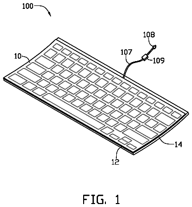
External touch keyboard
A touch keyboard includes a touch panel, a light guide plate, a keyboard layer, and a controller.
US 8,599,165 B2 · Assignee: Perceptive Pixel Inc. · Inventors: Westhues; Jonathan et al.
Sheet 1 of 8 from the published document. All sheets in the USPTO PDF
Methods, systems, and apparatus relate to touch sensors that are configured to measure a true capacitive touch and a force applied to the sensor from a user. Some implementations involve the measurement of force and true capacitive touch simultaneously in a touch capacitive sensor.
Touch sensors, such as those are used in touch screens for portable devices and for monitors, are configured to detect changes in capacitance to generate electrical signals based on the detected changes, and to send the generated electrical signals to a receiver for further processing.
1 of 8 drawing sheets so far from the published document, cropped to the drawing. Every sheet is in the USPTO PDF.
What the patent claimed, word for word. All of it is now free to use.
This disclosure relates to techniques for measuring capacitance in capacitive touch sensors, for example, in the measurement of force and true capacitive touch simultaneously in a sensor.
Touch sensors, such as those are used in touch screens for portable devices and for monitors, are configured to detect changes in capacitance to generate electrical signals based on the detected changes, and to send the generated electrical signals to a receiver for further processing.
This specification describes technologies generally relating to touch sensors that are configured to measure a true capacitive touch and/or a force applied to the sensor from a user.
In general, some aspects of the subject matter described in this specification can be embodied in methods that involve a sensor. Other embodiments of this aspect include corresponding systems, apparatus, and computer programs, configured to perform the actions of the methods, encoded on computer storage devices.
In general, another aspect of the subject matter described in this specification can be embodied in methods that include the actions related to a capacitive touch sensor. The sensor includes a first array (e.g., repetitive line patterns or an orderly arrangement of lines) of conductors arranged in rows, where the conductors in the first array are arranged substantially in parallel with one another. The sensor includes a second array of conductors arranged in columns, where columns of conductors in the second array are arranged substantially in parallel with one another. The columns of conductors in the second array are located underneath the first array of conductors, and the conductors in the second array are arranged in a direction that is substantially perpendicular to a direction of rows of conductors in the first array. The sensor includes a sheet having a dielectric material, where the sheet is located underneath the second array of conductors. The sensor includes a ground plane located underneath the sheet. The first and second arrays are configured to produce an electric field with electric field lines that extend in a first direction towards a user of the sensor and in a second direction towards the ground plane.
These and other embodiments can each optionally include one or more of the following features. A width of the conductors measured across a single row in the first array can be less than a distance of separation measured between adjacent edges of two adjacent rows of the first array, and a width of the conductors measured across a single column in the second array can be less than a distance of separation measured between adjacent edges of two adjacent columns in the second array. The ground plane can be positioned at least to partially terminate some of the electric field lines extending in the second direction. The sensor can be configured to detect an interruption in the electric field lines in the first direction. The sensor can be configured to detect the interruption of the electric field lines resulting from an object that is placed within a proximity of the sensor within the electric field lines of the first direction. The object can be a finger or some other body part of a user of the sensor. The sensor can include transmitters and receivers. The sensor can be configured to perform the following operations: transmit, with the transmitters, signals at least at two different frequencies on the first or second array of conductors; receive, with the receivers, the signals at least at the two different frequencies on the other of the first or second array of conductors; estimate a capacitance value at each of the two different frequencies using the received signals; determine that the object is the finger or some other body part of the user if the estimated capacitance values at the two frequencies differ by a factor of two or more; and determine that the object is not an object capable of generating a true capacitive touch signal (e.g., a finger or some other human body part) and an actuation of the sensor is due to measured force if the estimated capacitance values at the two frequencies do not differ by the factor of two or more. The sensor can be configured to receive an external force from touching or depressing the sensor. The sensor can be configured to compress at least the conductors in the first and second arrays toward the ground plane upon receiving the external force, and the sensor also can be configured to decrease a capacitance of the sensor when the external force is applied to the sensor. The sensor can include a capacitance characteristic where a level of measured capacitance decreases monotonically from when an object is placed within proximity of the sensor to when the object touches and depresses the sensor. The ground plane can include a sheet of indium tin oxide (ITO) or a transparent conductor. The ground plane can include wires or metal formed on a liquid crystal display (LCD). The sensor can be configured such that either one of the ground plane or a second sheet of material is formed underneath the sheet having the dielectric material, where the second sheet of material includes a dielectric constant that is higher than that of the deformable dielectric material. The sensor can be configured such that either the ground plane can be formed underneath the sheet having the deformable dielectric material or a second sheet of material can be formed above the sheet having the deformable dielectric material, for which the second sheet of material can have a dielectric constant that is higher than the sheet of the deformable dielectric material. The sensor can include indium tin oxide (ITO) on a polyester sheet (PET). The sensor can have opaque metal traces on a polyester sheet (PET) or a plastic substance. The conductors can include a transparent conductive material arranged in a pattern to produce a fringing electric field between the first and second array of conductors. The rows and columns can include diamond-shaped patterns at non-intersecting locations of the conductors of the first and second arrays. The conductors in the second array can be positioned between the first array of conductors and the deformable dielectric, and the deformable dielectric can be positioned between the conductors in the second array and the ground plane.
In general, another aspect of the subject matter described in this specification can be embodied in methods that include the actions related to a capacitive touch sensor. The sensor includes a first array of conductors arranged in rows, where the rows of conductors in the first array are arranged substantially in parallel with one another, and a width of the conductors measured across a single row in the first array is less than a distance of separation between respective conductors measured between adjacent edges of two adjacent rows of the first array. The sensor includes a second array of conductors arranged in columns, where the columns of conductors in the second array are arranged substantially in parallel with one another, and where the conductors in the second array are located underneath the conductors in the first array. The conductors in the second array are arranged in a direction that is substantially perpendicular to a direction of first array of conductors, and a width of the conductors measured across a single column in the second array is greater than a distance of separation between respective conductors measured between adjacent edges of two adjacent columns in the second array. The sensor includes a sheet having a dielectric material, where the sheet is located underneath the second array of conductors. The sensor includes a third array of conductors arranged in rows, where the rows of conductors in the third array are arranged substantially in parallel with one another, and the conductors in the third array are located underneath the sheet. The rows of conductors in the third array are arranged in a direction that is substantially perpendicular to a direction of the columns of conductors in the second array and a width of the conductors measured across a single row of the third array is greater than a distance of separation between respective conductors measured between adjacent edges of two adjacent rows in the third array.
These and other embodiments can each optionally include one or more of the following features. The sensor can include a force-sensitive sensor and a true capacitive touch sensor, where the true capacitive touch sensor can include the conductors of the first and second arrays, and the force-sensitive sensor can include the conductors of the second and third arrays and the sheet having the dielectric material. The force-sensitive sensor can be configured for a first measurement of a first capacitance for a parallel-plate capacitance between intersections of the conductors of the second and third arrays, and the true capacitive touch sensor can be configured for a second measurement of a second capacitance related to a fringing electric field between the first and second arrays of conductors. The sensor can be configured to detect if an object is within proximity of touching the sensor by the fringing electric field. The sensor can be further configured to detect if an object touches or applies a force to the sensor. The sensor can be configured to decrease a level of the second capacitance as the object moves closer to touching the sensor. The sensor can be configured to increase a level of the first capacitance as the object touches and applies the force to the sensor. The sensor can include indium tin oxide (ITO) on a polyester sheet (PET). The sensor can include opaque metal traces on a polyester sheet (PET) or a plastic substance. The conductors can include a transparent conductive material arranged in a pattern to produce a fringing electric field between the first and second array of conductors. The conductors in the second array can be positioned between the first array of conductors and the deformable dielectric, and the deformable dielectric can be positioned between the conductors in the second array and the third array of conductors.
In general, another aspect of the subject matter described in this specification can be embodied in methods that include the actions related a capacitive touch sensor. The sensor includes a first array of conductors arranged in rows, a second array of conductors arranged in columns that are substantially perpendicular to the rows of conductors in the first array, at least one transmitter coupled to the conductors within one of the first or second array of conductors, and at least one receiver coupled to the conductors within the other of the first or second array of conductors. A method for conducting measurements in the sensor involves transmitting, with the at least one transmitter, signals at least at two different frequencies that generate an electric field between at least one of the conductors in the first array and at least one of the conductors in the second array, for which the first and second arrays are configured to produce a fringing electric field that extends in a direction towards a user of the sensor and to enable detection of an interruption of the electric field resulting from an object that is placed within a proximity of the sensor. The method involves receiving, with the at least one receiver, the signals with the two or more different frequencies, estimating a capacitance value at each of the two or more different frequencies using the received signals, and determining if the estimated capacitance value at each of the two or more frequencies differs by a factor of about two or more. The method involves computing a ratio between the estimated capacitance values, and comparing the ratio against a threshold, for which the threshold comprises a value that is approximately two. The method may also involve computing a difference between the estimated capacitance values, and comparing the difference against a threshold. The method involves determining whether the object is capable of generating a true capacitive touch signal (e.g., a finger or some other human body part) and whether an actuation of the sensor is due to measured force based on results of the comparison of the ratio or difference between the estimated capacitance values at the two or more frequencies.
These and other embodiments can each optionally include one or more of the following features. The method can involve determining that the object is a finger or some other human body part of a user of the touch sensor if the estimated capacitance values at the two frequencies differ by the factor of about two or more. The conductors in the first array can be arranged substantially in parallel with one another, and the conductors in the second array can be arranged substantially in parallel with one another. The conductors in the second array can be located underneath the conductors in the first array. A width of the conductors measured across a single row the first array can be less than a distance of separation between respective conductors measured between adjacent edges of two adjacent rows of the first array, and a width of the conductors measured across a single column the second array can be less than a distance of separation between respective conductors measured between adjacent edges of two adjacent columns in the second array. The sensor can include a sheet having a dielectric material, where the sheet can be located underneath the second array of conductors; and the sensor can include a ground plane located underneath the sheet. With regards to the frequencies, at least the two different frequencies can differ by a ratio of approximately four to one. The sensor can include a true capacitive touch sensor. The sensor can include a force-sensitive sensor and a true capacitive touch sensor, for which the true capacitive touch sensor can include the conductors in the first and second arrays, and the force-sensitive sensor can include the conductors in the second array, conductors in a third array and a sheet having a dielectric material. The conductors in the first array can be arranged substantially in parallel with one another. The width of the conductors measured across a single row in the first array can be less than a distance of separation between respective conductors measured between adjacent edges of two adjacent rows of the first array. The conductors in the second array can be arranged substantially in parallel with one another. The conductors in the second array can be located underneath the conductors of the first array. The width of the conductors measured across a single column in the second array can be greater than a distance of separation between respective conductors measured between adjacent edges of two adjacent columns in the second array. The sheet can be located underneath the conductors of the second array. The conductors of the third array can be arranged in rows, and the conductors in the third array can be arranged substantially in parallel with one another. The conductors in the third array can be located underneath the sheet. The conductors in the third array can be arranged in a direction that is substantially perpendicular to a direction of conductors in the second array, and a width of the conductors measured across a single row in the third array can be greater than a distance of separation between respective conductors measured between adjacent edges of two adjacent rows in the third array. The two different frequencies can include a first frequency and a second frequency, and the first frequency can be higher than the second frequency. The method also can include receiving signals for the second frequency at the at least one receiver that has a higher current than the signals received for the first frequency. The sensor can include indium tin oxide (ITO) on a polyester sheet (PET). The sensor can have opaque metal traces on a polyester sheet (PET) or a plastic substance. The conductors can have a transparent conductive material arranged in a pattern to produce a fringing electric field between the first and second array of conductors. The rows and columns can have diamond-shaped patterns at non-intersecting locations of the conductors of the first and second arrays.
The details of one or more embodiments of the subject matter described in this specification are set forth in the accompanying drawings and the description below. Other features and aspects of the subject matter will become apparent from the description, the drawings, and the claims.
FIG. 1 depicts a diagram of an array of rows and columns for a touch sensor.
FIG. 2 depicts a diagram of another example of an array of rows and columns for a touch sensor.
FIG. 3 depicts a diagram of a graph of measured capacitance versus a perceived touch force or proximity signal received by the touch sensor of FIG. 2.
FIG. 4 depicts a diagram of an array of rows and columns for a touch sensor.
FIG. 5 depicts a diagram exemplifying fringing fields that exist around a row and a column of the touch sensor of FIG. 4.
FIG. 6 depicts a diagram of a graph of measured capacitance versus a perceived touch force or proximity signal received by the sensor.
FIG. 7 depicts a diagram of a hybrid touch sensor.
FIG. 8 depicts a diagram of an array of rows and columns for the touch sensor, where the rows and columns have a diamond pattern.
Like reference numbers and designations in the various drawings indicate like elements.
In a capacitive touch screen, sensors are made from electrically conductive rows and columns, where the rows and columns are movable to receive a force applied from a user of the sensor. The rows and columns cross over each other, approximately perpendicular, and form a two-dimensional matrix. The electronic controller for such a touch screen will measure the capacitance from each row to each column at each intersection, producing m*n measurements for a matrix with m rows and n columns. The capacitance is measured by applying a time-varying excitation voltage on each conductor (which we will assume here, arbitrarily, to be a column), and measuring the current coupled into each row. Multiple rows are measured in parallel, and the process is repeated serially for each column, or partially in parallel, with orthogonal excitation waveforms used on multiple columns. For example, orthogonal excitation waveforms may be used on the multiple columns, as described in U.S. patent application Ser. No. 12/838,419, filed Jul. 16, 2010, which is incorporated by reference in its entirety.
If the user's finger is moved close to one of the intersections, then the capacitance at that intersection will change. The user's finger is conductive, has dielectric constant different from that of air, and, to the extent that it is conductive, has some connection through the user's body to the controller circuit's ground node. Some combination of these effects will cause a change in the capacitance, which may decrease (as current flows from the transmitter into the user's body and to ground, instead of from the transmitter to the receiver) or increase (as current flows from the transmitter into the user's finger, and from the user's finger into the receiver; the user's finger is more conductive and has higher dielectric constant than air). The mode in which the user's finger causes a decrease in the capacitance occurs at higher frequencies, which allows for more total energy transferred in a given integration period, which allows for higher signal-to-noise ratio (SNR). The decreasing mode is therefore used whenever true capacitive touch is measured in this disclosure.
The "true capacitive touch" measurement is used because it has zero actuation force. It responds to the position of the user's touch, not the force, and therefore responds to even a very light touch. In some applications, however, an analog measurement of the user's touch force provides a useful additional degree of freedom.
For example, force may be mapped to capacitance by constructing a parallel-plate capacitor with a deformable dielectric between the plates. When a force is applied to the capacitor, the dielectric material deforms, and allows the plates to move closer together. This increases the measured capacitance. A matrix of such sensors can be constructed, for example with wide, overlapping rows and columns, and a dielectric material between the rows and columns. This matrix may be scanned in the same way as to measure true capacitive touch. The force-sensitive sensor designs also allow the device to be actuated with objects other than the finger, such as with a stylus instrument, e.g., a hard plastic rod. Anything that can be used to apply force (including, for example, a non-conductive plastic object) can be used for providing a signal corresponding to the force of the sensor. An example of such a sensor is reproduced as FIG. 1.
Within the array of rows and columns for touch sensor 100 shown within FIG. 1, the touch sensor 100 includes transparent, electrically conductive rows and columns. The touch sensor 100 has row conductors 130 formed over a deformable dielectric 110. The deformable dielectric 110 is formed atop column conductors 120. These conductors may be made from indium tin oxide (ITO), but other materials may also be used, such as silver nano-wires, or larger-scale metal wires that are slightly or largely opaque but small enough to be relatively inconspicuous. The illustrated configuration yields conductors arranged in a two-dimensional orthogonal matrix, for example, with row conductors being substantially parallel to an x-axis, and column conductors being substantially parallel to a y-axis.
Touch sensor 100 includes wide columns and wide rows that overlap, yielding a parallel-plate capacitance at the areas of the overlap between the rows and columns. In FIG. 1, the dielectric 110 is deformable, and the rows and columns are positioned on flexible pieces of indium tin oxide (ITO) on a polyester sheet, for example. When touch sensor 100 receives force applied by an external force, such as by a user's finger, dielectric 110 deforms and decreases the separation between the rows and columns in the depressed area, causing the measured capacitance increases in that area. The capacitance of the matrix of rows and columns can be read out to measure the capacitance at each of the m*n intersections, independently. In FIG. 1, the electric field is within the row and columns, so the sensor primarily responds to a force applied to the sensor. The force may include a physical depression in the sensor resulting from a touch from a user's finger or from some other conductive or non-conductive object, such as a stylus instrument or some other non-conductive object.
In another architecture, instead of measuring the capacitance from each row to each column, it is possible to measure the capacitance from each row or column to ground. In a system employing this design with m rows and n columns, m+n measurements are made, not m*n. In this case, the parallel plate capacitance would occur between the row or column and the ground plane, not between the row and the column. Adopting this architecture, a force that is applied at more than one point may generate a result that is not unique to the locations where the force is applied. For example, forces at positions (1, 2) and (3, 4) will generate increased capacitance on rows 1 and 3, and columns 2 and 4; but forces at positions (1, 4) and (3, 2) will also generate increased capacitance on those same rows and columns. Heuristic methods may be employed to thereafter attempt to resolve among competing potential source locations for the inspiring force, for example, by considering the sequence in which the points are touched. The m*n architectures discussed below, however, do not have to employ heuristic methods to resolve among competing potential source locations for the inspiring force. The features described below can offer m*n architectures that provide correct results when two points are touched almost simultaneously, or when points move so that they lie along a horizontal (parallel to the rows) or vertical (parallel to the columns) line.
In FIG. 2, touch sensor 200 is shown having an array of rows and columns. The touch sensor 200 has transparent, electrically conductive rows and columns. The touch sensor 200 has row conductors 230 positioned over a deformable dielectric 110. The deformable dielectric 110 is positioned above column conductors 120. For reasons described below, the touch sensor 200 of FIG. 2 has relatively narrow row conductors 230 with relatively wide spaces between each of the row conductors.
The FIG. 2 structure produces both the above-noted parallel-plate capacitance, and a fringing capacitance that may be interrupted by the user's finger. Such a structure measures both true capacitive touch, from the fringing field, and force, from the parallel-plate capacitance, as the material between the row and column deforms. Such a structure orients the top conductors in relatively sparse relative orientation, with space between them to allow the field to fringe up; an example of this structure appears as FIG. 2, but other structures are also contemplated with this property. For example, a diamond pattern 800, as shown in FIG. 8, may be configured to have this property, using the fringing field between the diamonds and the parallel-plate capacitance where the rows 820 and columns 830 cross over one another, or an interdigitated pattern.
In FIG. 2, the row conductors 230 are narrow instead of wide so that there is a large spacing between the row conductors 230 to reduce an amount of parallel plate capacitance between the row conductors 230 and the column conductors 120, and to allow a fringing field from the row conductors 230 to form so that a disruption of the fringing field can be detected by the sensor to provide for a fringing capacitance for a touch (non-force) signal. Other implementations may be configured like FIG. 2, for example, the diamond pattern 800 in FIG. 8 or interdigitated patterns.
As described, the touch sensor 200 of FIG. 2 can serve as both a "true capacitive touch sensor" and "a force-sensitive sensor," respectively, measuring changes to the fringing field and the electric field in the dielectric. For instance, as a force-sensitive sensor, touch sensor 200 operates similarly to the touch sensor 100 of FIG. 1, where a parallel-plate capacitance is measured resulting from a force applied to the touch sensor, providing an additional degree of freedom. For example, with a user's finger, an amount of force applied by the user for the touch can provide the additional degree of freedom, such as having a light touch to indicate one type of instruction and a harder touch to indicate another type of instruction. Force-sensitive sensor designs can also allow touch sensor 200 to be actuated with objects other than the finger, such as with a stylus instrument (e.g., a hard plastic rod, or any conductive or non-conductive object) for providing a signal corresponding to the force for the sensor. For applied force with a relatively small contact area, for example, the force may be measured entirely at one intersection in the matrix, and that measurement may be proportional to the force applied. For applied force with a relatively large contact area, for example, the force may be measured at multiple intersections in the matrix, and those measurements may be proportional to the integral of that force over the area of each particular intersection, and therefore to the applied pressure. In this disclosure, the terms for force and pressure may be used interchangeably. In some implementations, the signal produced by the force in the touch sensor may be an analog measurement of the user's touch force.
By contrast, and as earlier indicated, operating as a "true capacitive touch sensor," touch sensor 200 generates measurements despite the absence of force. In this sense, true capacitive touch is measured by the disruption in the electric field when a user's finger is brought into proximity with or interferes with the fringing field of the sensor. Thus, true capacitive touch signal is generated in the touch sensor 200, even if the user does not apply pressure to the sensor, since a measurable change in the capacitance can be determined when a user's finger is brought into proximity with the fringing field of the sensor. Since the user does not have to apply a force to actuate the sensor, there is no resulting frictional force if the user's finger moves within the plane of the sensor, and the user does not feel this undesirable frictional drag on the user's finger. Rather, the true capacitive touch sensor can respond to the position of the user's finger, not the force, and therefore can respond to even a very light touch from a user.
In FIG. 3, measured capacitance 310 is related to a perceived touch force based on a corresponding proximity signal 320 received by the touch sensor 200 of FIG. 2. Specifically, as demonstrated by FIG. 3, as the user's finger approaches the touch sensor of 350, causing the measured capacitance 310 to progressively decrease as the user's finger will interrupt the fringing field from a row to a column. The capacitance due the fringing field is the dominant capacitance in this instance. After a point where the user's finger touches the sensor 360 and begins to apply an increasing force of 370, the capacitance increases as the parallel plate capacitance increasingly becomes the dominant capacitance. This represents a non-monotonic transfer function from measurements of the perceived touch force to capacitance. As a consequence of the non-monotonic transfer function depicted by FIG. 3, a user that touches and presses hard enough on the touch sensor may increase the measured parallel-plate capacitance to the point where that parallel-plate capacitance offsets a decrease in the measured capacitance corresponding to that user's interaction on the fringing capacitance effects, and yielding results that obfuscate whether the user touches or attempts to touch the sensor at all.
There may be other measurements performed in other implementations of touch sensors. For example, in some other implementations, the capacitance can be measured from each row and column to ground, instead of from each row to each column, thus making m+n measurements instead of m*n measurements. In this case, the parallel plate capacitance would occur between the row or column and the ground plane, not between the row and the column. Some of these touch sensor implementations employing the m+n measurements may not be able to determine each force independently (or their locations) when force is applied at more than one point, even with complex modeling and computations.
As earlier mentioned, when the user touches the capacitive touch sensor, at least two different effects are observed. First, some of the energy flowing out of the transmitter can flow into the user and return to ground through the user's stray capacitance to that node. This stray capacitance may occur, for example, if the user is holding the device's metal case, even through a non-conductive coating, or, failing that, through the user's finger, because the sensor pitch can be fine enough so that their finger can also be close to other elements in the matrix, for which some elements will be grounded. This first effect may decrease the total energy that flows to the receiver. Second, some of the energy flowing out of the transmitter can couple into the user's finger, through the user's flesh, and then out of the user's finger to the receiver. Because the dielectric constant of the user's finger, which is approximately the same as salt water, is larger than that of air, this can increase the coupling effect, and increase the received energy.
The two effects can produce different responses for the energy flow. For example, depending on which effect dominates, there may be a non-monotonic relationship between the measured signal and the distance from the user's finger to the sensor. With this in mind, to improve performance of the sensor, touch sensors can be configured to operate in either a strictly-increasing or a strictly-decreasing mode to have a monotonic relationship. The strictly-decreasing mode may work particularly well in some implementations because this mode may occur at higher frequencies. The effects corresponding to the strictly-decreasing mode may also occur with a greater separation between the user's finger and the touch sensor (since as the user's finger becomes very close to the sensor, the effect in which current couples from a transmitter, to the user's finger, and then through the user to a receiver dominates, and causes an increased capacitance). This can allow a larger thickness for the glass for the cover of the sensor. Some other implementations, however, may use the strictly-increasing mode. As described below, there may be other effects on the mode that are a function of frequency.
As illustrated through the example shown in FIG. 4, in some implementations, it is possible to arrange a sensor such that a first fringing capacitance is affected by force, and a second and different fringing capacitance can be affected by the user's finger. This arrangement can be accomplished using a pattern of electrodes that generates a significant fringing field on both the front (toward the user) and back (toward the display) sides of the sensor. A pattern with narrow wires can have this property, for example, as does a diamond 800 pattern (FIG. 8), or an interdigitated pattern, or others. The sensor can include a flexible material, for example, metal or transparent conductive (e.g., indium tin oxide, ITO) traces on polyester (PET) or other plastic film substrate. The sensor may be placed above a ground plane, separated by a deformable dielectric material.
In particular, in FIG. 4, there are narrow row conductors 420 and narrow column conductors 430 with wide spaces between each of the rows 420 and between each of the columns 430. The touch sensor 400 includes row conductors 420 above the column conductors 430. Below the column conductors 430 is a deformable dielectric 110 with a ground plane 440 underneath. The column conductors 430 are positioned between the row conductors 420 and the deformable dielectric 110, and the deformable dielectric 100 is positioned between the column conductors 430 and the ground plane 440. In terms of the perspective illustrated in FIG. 4, the row conductors 420 are considered to be on top of the other layers shown for the sensor, and the ground place 440 is considered to be underneath the other layers shown for the sensor. The dominant capacitance in FIG. 4 can be fringing capacitance between the respective rows 420 and columns 430. Since the rows 420 and columns 430 can be roughly coplanar (e.g., the separation between the rows and columns is relatively small), the fringing field can be roughly symmetric.
FIG. 5 illustrates exemplary fringing field lines 540 around a row conductor 420 and a column conductor 430 of the touch sensor 400 of FIG. 4. In FIG. 5, the fringing field lines 540 can be symmetric on both sides of the row conductor 420 and column conductor 430, where on one side, fringing field lines 540 extend out from the touch sensor 400 toward a user, and on another side, fringing field lines 540 extend out away from the user (e.g., on a back side and/or towards a display). The fringing field on the front side of the touch sensor can be disrupted by the user's finger and provide a true capacitive touch signal, which tends to decrease the measured capacitance. The fringing field on the back side of the sensor can be utilized by the deformable dielectric 110 and a ground plane 440. If the touch sensor is pressed with a non-conductive object then the conductors 420, 430 are moved toward the ground plane 440, causing a fraction of the fringing field on that back side of the sensor to be shorted or at least partially terminated by the ground plane 440. The current flowing into the transmitter therefore flows, at least in part, into the ground plane 440, which decreases the measured capacitance slightly, relative to the capacitance measured if that ground plane was not present.
In FIG. 6, measured capacitance 610 is related to a perceived touch force based on a corresponding proximity signal 620 received by the touch sensor. As the user's finger approaches the touch sensor 640 the measured capacitance 630 decreases. As the user begins to touch the sensor 650 the capacitance decreases, and as the user's finger is applied with an increased force 660, the capacitance further decreases as the sensor moves close to the ground plane.
Specifically, if the user's finger presses very lightly, the capacitance decreases because the current that flows out of the transmitter of the sensor can flow at least partially through the user's finger to ground, based on the at least partial connection to circuit ground of the user, instead of flowing into the receiver of the sensor. If the user's finger presses with increased force, then the measured capacitance decreases further because the rows and columns of the sensor can move closer to the ground plane, which causes the separate but complimentary effect of having some of the current flow into the ground plane instead of the receiver.
The measurement of the capacitance illustrated by FIG. 6 is therefore monotonic with respect to the user's perceived touch force. The monotonic capacitance characteristic can allow a mapping of the function of the capacitance to a user's finger movement and/or a measurement of pressure.
Techniques employing frequency can be used to distinguish between the sensing of the capacitance resulting from the user's finger and the capacitance resulting from the force applied by some other object (e.g., a stylus instrument, a conductive or non-conductive object). For example, the capacitance with respect to a user's finger can vary with frequency, and the capacitance due to the field within the deformable dielectric can stay approximately constant with frequency. By assessing the capacitive measurements at different frequencies, a determination can be made as to whether the touch sensor is touched by the user's finger or the non-conductive object.
The description continues in the full USPTO document.
About 6,338 words. The USPTO PDF has it with every drawing.
Fees are due 3.5, 7.5 and 11.5 years after grant. This patent expired on December 3, 2025, so the fee marked "not paid" was the one that went unpaid.
FORCE AND TRUE CAPACITIVE TOUCH MEASUREMENT TECHNIQUES FOR CAPACITIVE TOUCH SENSORS
Filed Aug 2010 · published Feb 2012Force and true capacitive touch measurement techniques for capacitive touch sensors
Filed Aug 2010 · granted Dec 2013Earlier publications, parents and continuations. None of them can still be enforced, or this patent would not be listed.
Prior art cited by the examiner or applicant. Useful when you check your own idea for novelty.
Everything on this page comes from the documents linked above.


