Lapsed, fee not paid79 drawings
Cameras, Displays & Optics · US 8,599,109 B2
Display device and driving method thereof
Each pixel of a display device has a current supply circuit, a switch portion, and a light emitting element.
US 8,599,121 B2 · Assignee: Sharp Kabushiki Kaisha · Inventors: Yamada; Takaharu
Sheet 1 of 17 from the published document. All sheets in the USPTO PDF
An active matrix substrate used in a display device or the like capable of making substantially uniform the level shift generated in the pixel potential caused by the distribution of resistance and capacity in each signal line is disclosed. On the TFT substrate which is an active matrix substrate including a common electrode line formed parallel to the scan signal line, in order to eliminate non-uniformity of the level shift of the pixel potential generated at the scan signal fall, each pixel circuit is formed so that the capacity between the scan signal line and the pixel electrode becomes greater as electrically going farther from the scan signal line drive circuit and going farther from the common electrode line drive circuit. Embodiments can be applied especially to an active matrix substrate used in a liquid crystal display device, an EL display device, and the like.
Active matrix substrates are used widely in active matrix type display devices such as liquid crystal display devices and EL display devices, as well as in a variety of active matrix type sensors and other products. In particular, special attentions are being paid to liquid crystal display devices in which each display pixel is provided with a switching element such as a thin-film transistor (hereinafter abbreviated as TFT) which is a type of field-effect transistors, since these display devices are capable of displaying excellent images without crosstalk between mutually adjacent display pixels even if there is a large number of display pixels. Such an active matrix type liquid crystal display device primarily includes a liquid crystal display panel and a drive circuit for the panel. The liquid crystal display panel includes a pair of electrode substrates sandwiching a liquid crystal la
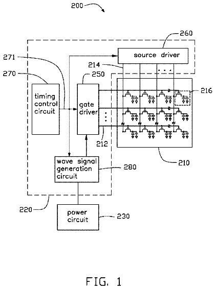
1 of 17 drawing sheets so far from the published document, cropped to the drawing. Every sheet is in the USPTO PDF.
What the patent claimed, word for word. All of it is now free to use.
The present invention relates to active matrix substrates and drive circuits for the substrates used in matrix type liquid crystal display devices, EL (Electroluminescence) display devices and so on. More specifically, the present invention relates to an active matrix substrate formed with a plurality of data signal lines and a plurality of scanning lines to cross with each other in a grid pattern and a matrix of pixel circuits each including a switching element provided by a field-effect transistor such as a thin-film transistor and a voltage holding capacitor. The invention also relates to a drive circuit for the substrate.
Active matrix substrates are used widely in active matrix type display devices such as liquid crystal display devices and EL display devices, as well as in a variety of active matrix type sensors and other products. In particular, special attentions are being paid to liquid crystal display devices in which each display pixel is provided with a switching element such as a thin-film transistor (hereinafter abbreviated as TFT) which is a type of field-effect transistors, since these display devices are capable of displaying excellent images without crosstalk between mutually adjacent display pixels even if there is a large number of display pixels.
Such an active matrix type liquid crystal display device primarily includes a liquid crystal display panel and a drive circuit for the panel. The liquid crystal display panel includes a pair of electrode substrates sandwiching a liquid crystal layer. Each electrode substrate has its outer surface covered by a polarizer.
Of the pair of electrode substrates, one is an active matrix substrate called TFT substrate. The TFT substrate includes an insulating substrate made of glass for example, formed with a plurality of data signal lines and a plurality of scanning signal lines crossing with each other in a grid pattern and in addition, a plurality of common electrode lines are formed to extend in parallel to the scanning signal lines. Further, correspondingly to each of the intersections made by the data signal lines and the scanning signal lines, a matrix of pixel circuits are formed. Each pixel circuit includes a pixel electrode for a corresponding pixel that serves to form images to be displayed, pixel capacities formed by the pixel electrode and other elements such as an opposed electrode which will be described later, and a TFT which serves as a switching element. The other electrode substrate, called opposed substrate, is provided by a transparent insulating substrate made of glass for example, having its entire surface laminated with a layer of opposed electrode and then with an alignment film.
The active matrix type liquid crystal display device includes, as a drive circuit for the liquid crystal display panel configured as the above, a scanning signal line drive circuit connected with the scanning signal lines, a data signal line drive circuit connected with the data signal lines, a common electrode line drive circuit connected with the common electrode lines, and an opposed electrode drive circuit connected with the opposed electrode.
The data signal line drive circuit generates, based on image signals received from an outside signal-source for example, a plurality of data signals successively in the form of analog voltage representing pixel values in each horizontal scanning line of the image to be displayed in the liquid crystal display panel, and applies these data signals respectively to the data signal lines in the liquid crystal display panel. The scanning signal line drive circuit selects the scanning signal lines in the liquid crystal display panel sequentially for each horizontal scanning period, and applies an active scanning signal (a voltage for turning ON the TFTs in the pixel circuit) to the selected scanning signal line, in each frame period (each vertical scanning period) for displaying an image on the liquid crystal display panel. The common electrode line drive circuit and the opposed electrode drive circuit apply signals to the common electrode lines and the opposed electrode respectively; these signals give electric potentials that serve as baseline voltages for voltages to be applied to the liquid crystal layer of the liquid crystal display panel.
As described above, the data signal lines are supplied with respective data signals, the scanning signal lines are supplied with respective scanning signals, whereby the pixel electrode in each pixel circuit of the liquid crystal display panel is supplied with a voltage representing the value of the pixel for the image to be displayed, with the potential at the opposed electrode serving as the baseline voltage, and the supplied voltage is held at the pixel capacity in each pixel circuit. Thus, a voltage which equals to the potential difference between each pixel electrode and the opposed electrode is applied to the liquid crystal layer. By controlling optical transmittance based on the applied voltage, the liquid crystal display panel displays an image represented by the image signals received from e.g. an outside signal-source.
FIG. 19 is a circuit diagram which shows a configuration of a pixel circuit in a TFT substrate serving as an active matrix substrate used in a liquid crystal display device as described above. A pixel circuit P(i, j) corresponds to one of the intersections made by the data signal lines and the scanning signal lines, and includes: a TFT 102 which has a source electrode connected with a data signal line S(i) passing the corresponding intersection, and a gate electrode connected with a scanning signal line G(j) passing the same intersection; and a pixel electrode 103 connected with a drain electrode of the TFT 102. The pixel electrode 103 and the opposed electrode form a liquid-crystal capacity Clc. The pixel electrode 103 and a common electrode line CS(j) provided along the scanning signal line G(j) form a common-electrode capacity (may also called "supplemental capacity") Ccs, and the pixel electrode 103 and the scanning signal line G(j) form a parasitic capacity Cgd.
Hereinafter, reference will be made to FIG. 4-(A) through FIG. 4-(D), FIG. 9 and FIG. 19, to describe a conventional method of driving the above-described TFT substrate in a liquid crystal display device. As a matter of well known fact, liquid crystal displays need AC driving in order to reduce burning images on the screen and display deterioration. The following description of a conventional driving method will assume that a frame-inversion driving method which is a type of AC driving is used.
FIG. 4-(A) through 4-(D) are voltage waveform charts of various voltage signals Vg(j), Vs(i), Vcs, Vcom in the TFT substrate and a waveform of a potential of the pixel electrode (hereinafter may also called "pixel potential") Vd (i, j) in two consecutive frame periods, i.e. a first frame period TF1 and a second frame period TF2. As shown in FIG. 4-(A), in the first frame period TF1, a voltage serving as a scanning signal (hereinafter called "scanning voltage") Vgh is applied from the scanning signal line drive circuit to the gate electrode g (i, j) of the TFT 102 in a pixel circuit P(i, j). This turns ON the TFT 102 (into a conductive state), where a voltage serving as a data signal (hereinafter called "data signal voltage") Vsp applied from the data signal line drive circuit to the data signal line S(i) is supplied to the pixel electrode 103 via the source electrode and the drain electrode of the TFT 102. Thus, the data signal voltage Vsp becomes a positive-polarity voltage with respect to the opposed-electrode potential Vcom (=common electrode potential Vcs), and is written to a pixel capacity Cpix which is formed by the pixel electrode 103 and other electrodes. As shown in FIG. 4-(D), the pixel electrode 103 holds the pixel potential Vdp until a scanning voltage Vgh is applied in the next frame period, i.e. the second frame period TF2. As shown in FIG. 19, the pixel capacity Cpix for holding the pixel potential Vdp is made of the liquid-crystal capacity Clc, the common-electrode capacity Ccs and the parasitic capacity Cgd. Meanwhile, the opposed electrode is set to a predetermined opposed-electrode potential Vcom by the opposed electrode drive circuit. Therefore, the liquid crystal sandwiched between the pixel electrode and the opposed electrode makes a response in accordance with the potential difference between the pixel potential Vdp and the opposed-electrode potential Vcom, achieving a display of the image.
Likewise, as shown in FIG. 4-(A), in the second frame period TF2, upon application of the scanning voltage Vgh from the scanning signal line drive circuit to the gate electrode g(i, j) of the TFT 102 in the pixel circuit P(i, j), the TFT 102 is turned ON, where a data signal voltage Vsn which is applied from the data signal line drive circuit to the data signal line S(i) is supplied to the pixel electrode 103 via the source electrode and the drain electrode of the TFT 102. Thus, the data signal voltage Vsn becomes a negative-polarity voltage with respect to the opposed-electrode potential Vcom (=Vcs), and is written into the pixel capacity Cpix. The pixel electrode 103 holds the pixel potential Vdn until the scanning voltage Vgh is applied in the next frame period. Thus, the liquid crystal sandwiched between the pixel electrode and the opposed electrode makes a response in accordance with the potential difference between the pixel potential Vdn and the opposed-electrode potential Vcom, achieving a display of the image, in an AC driving of a liquid crystal.
As shown in FIG. 19, a parasitic capacity Cgd is unavoidably formed between the scanning signal line G(j) and the pixel electrode 103 in each pixel circuit P(i, j) as a nature of the configuration. Therefore, as shown in FIG. 4-(D), at the time when the active scanning signal voltage, i.e. the scanning voltage Vgh falls down to the non active scanning signal voltage, i.e. the scanning voltage Vgl (represented by a time point ta in the figure), a level shift .DELTA.Vd occurs in the pixel potential Vd due to the parasitic capacity Cgd. It should be noted here that in FIG. 4-(D), the level shift of the pixel potential Vd (i, j) in the pixel circuit P(i, j) in the first frame period (in the period when a positive voltage is applied to the liquid crystal layer) TF1 (or more accurately, a level shift at a time point tb which is a time point well after the time point ta) is indicated by a symbol ".DELTA.Vdp (i, j)" whereas the level shift of the pixel potential Vd (i, j) in the pixel circuit P(i, j) in the second frame period (the period when a negative voltage is applied to the liquid crystal layer) TF2 is indicated by a symbol ".DELTA.Vdn (i, j)". However, when there is no need to specifically clarify the pixel circuit or the frame period, these level shifts will be indicated by a common symbol ".DELTA.Vd" as used in the above (The same will apply hereinafter).
The level shift .DELTA.Vd which occurs in the pixel potential Vd due to the parasitic capacity Cgd which is formed unavoidably in the TFT 102 is expressed as follows: .DELTA.Vd=VgppCgd/Cpix Vgpp=Vgl-Vgh Cpix=C1c+Ccs+Cgd The level shift causes such problems as flickers in the displayed image and decreased quality of the displayed image. For this reason, occurrence of the level shift .DELTA.Vd as the above is not preferable for liquid crystal display devices which are supposed to achieve ever higher fineness and quality.
Meanwhile, there has been a number of methods (means) proposed for eliminating or reducing the level shift .DELTA.Vd as described above. For example, a method has been proposed in which a bias is given to the potential at the opposed electrode so that the level shift .DELTA.Vd caused by the parasitic capacity Cgd will be reduced in advance. Also, JP-A Hei 11-281957 Gazette (This corresponds to U.S. Pat. No. 6,359,607, the contents of which is incorporated herein by reference), discloses a method in which the level shift variation in the pixel potential is reduced by controlling the fall of the scanning signal. Further, JP-A 2001-33758 Gazette discloses a method in which the level shift variation in the pixel potential (electric potential of the pixel electrode) by connecting a plurality of variable power sources to the common electrode line. [Patent Document 1] JP-A 2002-202493 Gazette [Patent Document 2] JP-A 2001-33758 Gazette [Patent Document 3] JP-A Hei 11-281957 Gazette [Patent Document 4] JP-A Hei 11-84428 Gazette [Patent Document 5] JP-A Hei 10-39328 Gazette [Patent Document 6] JP-A Hei 5-232512 Gazette
Problems to be Solved by the Invention
However, in the manufacture of the TFT substrate as an active matrix substrate for use in liquid crystal display devices, it is difficult to form ideal signal lines which are free from signal propagation delay, on a transparent insulating substrate provided by glass for example. A certain degree of signal propagation delay is unavoidable.
For example, scanning signal lines formed on the TFT substrate must be treated as a distributed constant wire which has a wiring resistance, a wiring capacity, etc. This means that the signal lines have a signal propagation delay characteristic. Therefore, the voltage waveform of the scanning signal Vg(j) in a scanning signal line deforms with increasing distance from the point where the scanning signal Vg(j) is applied by the scanning signal line drive circuit (i.e. from the input end of the scanning signal Vg(j)). Hence, the absolute value |.DELTA.Vd| of the level shift .DELTA.Vd caused in the pixel potential Vd by the parasitic capacity Cgd decreases with increasing distance from the input end of the scanning signal Vg(j) in the scanning signal line.
As described, the level shift .DELTA.Vd has different values depending on the location of pixel circuit, and therefore not uniform in the screen (in the TFT substrate). Therefore, if the method of giving a bias to the potential Vcom of the opposed electrode in an attempt that the level shift .DELTA.Vd of the pixel potential Vd will be reduced in advance, it is not possible to achieve sufficient elimination of the flickers in the displayed image and display quality deterioration which are caused by the level shift .DELTA.Vd, by simply applying a uniform bias to the opposed electrode. Specifically, with increase in the screen size and in the level of fineness, non-uniformity of the level shift .DELTA.Vd grows to a level beyond the viability of the above-described method, becoming unable to provide sufficient AC driving to each liquid crystal block which corresponds to a pixel, leading to problems such as flickers in the displayed image, burning images on the screen due to DC components applied to the liquid crystal, and so on.
To this problem, Patent Document 1 (Japanese Patent Laid-Open No. 2002-202493 Gazette) discloses a liquid crystal display device in which power supply for the opposed electrode that faces the pixel electrode is provided at least at two locations, i.e. on the input end side and on the terminating end side of the scanning signal line, and opposed voltages are supplied to the above-mentioned at least two power supply sources so that the potential of the opposed electrode will increase from the input-end side toward the output-end side. However, such a configuration complicates the structure for driving the opposed electrode, and furthermore, results in increased power consumption due to the current flow between the two power supply sources for the opposed electrode.
Patent Document 2 (Japanese Patent Laid-Open No. 2001-33758 Gazette) discloses another method: Specifically, level shift variation in the pixel potential is reduced by connecting a plurality of variable power sources to the common electrode line. If this method is used, it is possible to relatively cancel the level shift, with potential variation of the electrode which is opposed to the pixel electrode. However, the method requires a plurality of variable power sources in order to drive the common electrode.
Further, Patent Document 3 (Japanese Patent Laid-Open No. Hei 11-281957 Gazette) disclose another method: Specifically, level shift variation of the pixel potential is reduced by controlling the fall of the scanning signal. If this method is to be used, a special drive circuit must be provided. Further, time for charging the pixel capacity must be reduced.
Patent Document 4 (Japanese Patent Laid-Open Hei 11-84428 Gazette (This corresponds to U.S. Pat. No. 6,249,325 and No. 6,504,585, the contents of which are incorporated herein by reference)) discloses a liquid crystal display device: Toward the goal of uniformalizing the level shift of the pixel potential, an arrangement is made so that the capacity between the gate electrode and the source electrode of the thin-film transistor (TFT) formed in the liquid crystal display panel will be smaller on the input side of the gate signal line, and greater on the side of terminating end. However, due to lack of consideration to variation in the amount of charge in e.g. the pixel capacity caused by the current flows in the TFT from the time when the gate signal starts to fall to the time when the signal completes the fall (details will be described later), it is not possible to achieve sufficient elimination of the level shift non-uniformity of the pixel potential by the disclosed arrangement alone.
As will be described later, the inventor of the present invention found that in order to eliminate the level shift non-uniformity of the pixel potential, consideration must be made to influences of the parasitic capacity between the scanning signal line and the common electrode line and influences of the signal propagation delay characteristic in the common electrode line. However, these influences are not considered in any of the conventional techniques including the technique disclosed in Patent Document 4 (Japanese Patent Laid-Open Hei 11-84428 Gazette), so the level shift non-uniformity of the pixel potential cannot be eliminated sufficiently for this reason, either. Further, Patent Document 5 (Japanese Patent Laid-Open Hei 10-39328 Gazette (This corresponds to U.S. Pat. No. 6,028,650, the content of which is incorporated herein by reference)) discloses a liquid crystal display device, in which each of the pixel electrodes is provided with a supplemental capacity arranged in such a way that its capacity value will decrease as the distance increases from the input end of the gate signal line connected with the pixel electrode. However, again, such an arrangement as the above cannot eliminate the level shift non-uniformity of the pixel potential, for the same reason.
It is therefore a first object of the present invention to provide an active matrix substrate in which the level shift caused in the pixel potential by the resistance and capacity distribution in each signal line is substantially uniformalized within the substrate. Further, a second object of the present invention is to provide a drive circuit which drives an active matrix substrate in such a way that the level shifts caused in the pixel potential by the resistance and capacity distribution in each signal line are substantially uniformalized within the substrate. Further, a third object of the present invention is to provide a display device capable of giving a high quality display of images by substantially uniformalizing the level shift in the pixel potential within the active matrix substrate thereby canceling display non-uniformity.
Means for Solving the Problems
A first aspect of the present invention provides an active matrix substrate which includes:
data signal lines each for one of data signals;
scanning signal lines crossing with the data signal lines; and
a matrix of pixel circuits each corresponding to one of intersections made by the data signal lines and the scanning signal lines.
Each pixel circuit includes:
a field-effect transistor having: a source electrode connected with one of the data signal lines that passes through a corresponding one of the intersections, directly or via a predetermined switching element and/or a capacity element; and a gate electrode connected with one of the scanning signal lines that passes through the corresponding intersection; the field-effect transistor assuming a conductive state upon application of a predetermined ON voltage while assuming a nonconductive state upon application of a predetermined OFF voltage, to the gate electrode based on the source electrode as a baseline; and
a voltage holding electrode connected with a drain electrode of the field-effect transistor, providing a predetermined voltage holding capacitor.
Each pixel circuit is formed so that a value given by an equation below will be substantially equal among the pixel circuits: (VgppCgd+.DELTA.Qd)/Cpix where Vgpp represents an amount of potential change at the gate electrode from a time when a gate signal, which is given to the gate electrode of the field-effect transistor via the scanning signal line, starts its transition from the ON voltage to the OFF voltage to a time when the transition is complete; Cgd represents an electrostatic capacity between the gate electrode and the drain electrode in the field-effect transistor; .DELTA.Qd represents an amount of charge which moves through the field-effect transistor to the voltage holding electrode from the time when the gate signal starts its transition from the ON voltage to the OFF voltage to the time when the transition is complete; and Cpix represents a sum of electrostatic capacities formed between the drain electrode of the field-effect transistor or the voltage holding electrode and other electrodes in each pixel circuit.
In the above-described configuration, an arrangement in order that the value given by the above-described equation will be substantially equal among the pixel circuits may be that only one setting on a parameter such as a characteristic of the TFT or one of the electrostatic capacities (various electrostatic capacities formed between the pixel electrode and other electrodes) is changed, or may be that changes are made on a selected combination of these parameters.
A second aspect of the present invention provides the active matrix substrate according to the first aspect of the present invention which further includes
a common electrode line disposed for formation of predetermined electrostatic capacities between itself and the voltage holding electrodes.
The charge amount .DELTA.Qd is determined, taking into account a parasitic capacity between the scanning signal line and the common electrode line and/or a signal propagation delay characteristic of the common electrode line.
It should be appreciated that often, the common electrode line is disposed in parallel to the scanning signal line; however, the present invention is not limited to this as long as a predetermined electrostatic capacity (an equivalent of the common-electrode capacity or the supplemental capacity) is formed between the line and the pixel electrode. Further, the common electrode line may ride on a plurality of scanning signal lines, or a plurality of data signal lines. A plurality of the common electrode lines may be provided per a pixel circuit or per a pixel electrode, or the common electrode line may be provided as a plate. The freedom in the configuration of common electrode lines as the above applies to all of the aspects to be described here below.
A third aspect of the present invention provides the active matrix substrate according to the first aspect of the present invention, wherein the electrostatic capacity Cgd in each pixel circuit is formed so that the value given by the equation (VgppCgd+.DELTA.Qd)/Cpix is substantially equal among the pixel circuits.
A fourth aspect of the present invention provides the active matrix substrate according the first aspect of the present invention, wherein one of the electrostatic capacities which are formed between the drain electrode of the field-effect transistor or the voltage holding electrode and other electrodes other than the electrostatic capacity Cgd between the gate electrode and the drain electrode of the field-effect transistor is formed in each pixel circuit so that the value given by the equation (VgppCgd+.DELTA.Qd)/Cpix is substantially equal among the pixel circuits.
A fifth aspect of the present invention provides the active matrix substrate according to the first aspect of the present invention, wherein the field-effect transistor in each pixel circuit has a channel length and a channel width so selected that the value given by the equation (VgppCgd+.DELTA.Qd)/Cpix is substantially equal among the pixel circuits.
A sixth aspect of the present invention provides an active matrix substrate which includes:
data signal lines each for one of data signals;
scanning signal lines crossing with the data signal lines;
a matrix of pixel circuits each corresponding to one of intersections made by the data signal lines and the scanning signal lines.
Each pixel circuit includes:
a field-effect transistor having: a source electrode connected with one of the data signal lines that passes through a corresponding one of the intersections, directly or via a predetermined switching element and/or a capacity element; and a gate electrode connected with one of the scanning signal lines that passes through the corresponding intersection; and a voltage holding electrode connected with a drain electrode of the field-effect transistor, providing a predetermined voltage holding capacitor.
An electrostatic capacity Cgd between the gate electrode and the drain electrode in the field-effect transistor increases whereas a rate of the increase of the electrostatic capacity Cgd decreases with an increasing electrical distance from a location of signal application for driving the scanning signal line which passes through the corresponding intersection.
A seventh aspect of the present invention provides an active matrix substrate which includes:
data signal lines each for one of data signals;
scanning signal lines crossing with the data signal lines; and
a matrix of pixel circuits each corresponding to one of intersections made by the data signal lines and the scanning signal lines.
Each pixel circuit includes:
a field-effect transistor having: a source electrode connected with one of the data signal lines that passes through a corresponding one of the intersections, directly or via a predetermined switching element and/or a capacity element; a gate electrode connected with one of the scanning signal lines that passes through the corresponding intersection; and a voltage holding electrode connected with a drain electrode of the field-effect transistor, providing a predetermined voltage holding capacitor.
An area of overlap between the electrode constituting the scanning signal line that passes through the corresponding intersection and the voltage holding electrode or the drain electrode of the field-effect transistor increases whereas a rate of the increase of the area decreases with an increasing electrical distance from a location of signal application for driving the scanning signal line which passes through the corresponding intersection.
An eighth aspect of the present invention provides an active matrix substrate which includes:
data signal lines each for one of data signals;
scanning signal lines crossing with the data signal lines; and
a matrix of pixel circuits each corresponding to one of intersections made by the data signal lines and the scanning signal lines.
Each pixel circuit includes:
a field-effect transistor having: a source electrode connected with one of the data signal lines that passes through a corresponding one of the intersections, directly or via a predetermined switching element and/or a capacity element; a gate electrode connected with one of the scanning signal lines that passes through the corresponding intersection; and a voltage holding electrode connected with a drain electrode of the field-effect transistor, providing a predetermined voltage holding capacitor.
A ratio L/W between a channel length L and a channel width W in the field-effect transistor increases whereas a rate of the increase in the ratio L/W decreases with an increasing electrical distance from a location of signal application for driving the scanning signal line which passes through the corresponding intersection.
A ninth aspect of the present invention provides an active matrix substrate which includes:
data signal lines each for one of data signals;
scanning signal lines crossing with the data signal lines; and
a matrix of pixel circuits each corresponding to one of intersections made by the data signal lines and the scanning signal lines;
Each pixel circuit includes:
a field-effect transistor having: a source electrode connected with one of the data signal lines that passes through a corresponding one of the intersections, directly or via a predetermined switching element and/or a capacity element; a gate electrode connected with one of the scanning signal lines that passes through the corresponding intersection; and a voltage holding electrode connected with a drain electrode of the field-effect transistor, providing a predetermined voltage holding capacitor.
At least one of the electrostatic capacities which are formed between the drain electrode of the field-effect transistor or the voltage holding electrode and other electrodes other than the electrostatic capacity Cgd between the gate electrode and the drain electrode of the field-effect transistor decreases while a rate of the decrease of said at least one electrostatic capacity decreases with an increasing electrical distance from a location of signal application for driving the scanning signal line which passes through the corresponding intersection.
A tenth aspect of the present invention provides an active matrix substrate which includes:
data signal lines each for one of data signals;
scanning signal lines crossing with the data signal lines;
a matrix of pixel circuits each corresponding to one of intersections made by the data signal lines and the scanning signal lines; and
a common electrode line disposed for formation of a predetermined electric capacity in each pixel circuit;
Each pixel circuit includes:
a field-effect transistor having: a source electrode connected with one of the data signal lines that passes through a corresponding one of the intersections, directly or via a predetermined switching element and/or a capacity element; a gate electrode connected with one of the scanning signal lines that passes through the corresponding intersection; and a voltage holding electrode connected with a drain electrode of the field-effect transistor, providing the predetermined electrostatic capacity between itself and the common electrode line.
An electrostatic capacity Cgd between the gate electrode and the drain electrode in the field-effect transistor increases with an increasing electrical distance from a location where an electric potential to be supplied to the common electrode line is applied to the common electrode line.
An eleventh aspect of the present invention provides an active matrix substrate which includes:
data signal lines each for one of data signals;
scanning signal lines crossing with the data signal lines;
a matrix of pixel circuits each corresponding to one of intersections made by the data signal lines and the scanning signal lines; and
a common electrode line disposed to form a predetermined electric capacity in each pixel circuit.
Each pixel circuit includes:
a field-effect transistor having: a source electrode connected with one of the data signal lines that passes through a corresponding one of the intersections, directly or via a predetermined switching element and/or a capacity element; a gate electrode connected with one of the scanning signal lines that passes through the corresponding intersection; and
a voltage holding electrode connected with a drain electrode of the field-effect transistor, providing the predetermined electrostatic capacity between itself and the common electrode line.
The pixel circuits include a first, a second and a third pixel circuits, the first pixel circuit is closer to an end of the common electrode line and farther from a center of the common electrode line than the second pixel circuit. The third pixel circuit is closer to another end of the common electrode line and farther from the center of the common electrode line than the second pixel circuit, and
an electrostatic capacity Cgd between the gate electrode and the drain electrode in the field-effect transistor in the second pixel circuit is greater than an electrostatic capacity Cgd between the gate electrode and the drain electrode in the field-effect transistor in both of the first and the third pixel circuits.
A twelfth aspect of the present invention provides an active matrix substrate which includes:
data signal lines each for one of data signals;
scanning signal lines crossing with the data signal lines;
a matrix of pixel circuits each corresponding to one of intersections made by the data signal lines and the scanning signal lines; and
a common electrode line disposed to form a predetermined electric capacity in each pixel circuit.
Each pixel circuit includes:
a field-effect transistor having: a source electrode connected with one of the data signal lines that passes through a corresponding one of the intersections, directly or via a predetermined switching element and/or a capacity element; a gate electrode connected with one of the scanning signal lines that passes through the corresponding intersection; and a voltage holding electrode connected with a drain electrode of the field-effect transistor, providing the predetermined electrostatic capacity between itself and the common electrode line.
An area of overlap between the electrode constituting the scanning signal line that passes through the corresponding intersection and the voltage holding electrode or the drain electrode of the field-effect transistor increases with an increasing electrical distance from a location where an electric potential to be supplied to the common electrode line is applied to the common electrode line.
A thirteenth aspect of the present invention provides an active matrix substrate which includes:
data signal lines each for one of data signals;
scanning signal lines crossing with the data signal lines;
a matrix of pixel circuits each corresponding to one of intersections made by the data signal lines and the scanning signal lines; and
a common electrode line disposed to form a predetermined electric capacity in each pixel circuit.
Each pixel circuit includes:
a field-effect transistor having: a source electrode connected with one of the data signal lines that passes through a corresponding one of the intersections, directly or via a predetermined switching element and/or a capacity element; a gate electrode connected with one of the scanning signal lines that passes through the corresponding intersection.
A voltage holding electrode connected with a drain electrode of the field-effect transistor, providing the predetermined electrostatic capacity between itself and the common electrode line.
The pixel circuits include a first, a second and a third pixel circuits, the first pixel circuit is closer to an end of the common electrode line and farther from a center of the common electrode line than the second pixel circuit. The third pixel circuit is closer to another end of the common electrode line and farther from the center of the common electrode line than the second pixel circuit, and
an area of overlap between the electrode constituting the scanning signal line that passes through the corresponding intersection and the voltage holding electrode or the drain electrode of the field-effect transistor in the second pixel circuit is greater
than an area of overlap between the electrode constituting the scanning signal line that passes through the corresponding intersection and the voltage holding electrode or the drain electrode of the field-effect transistor in the first pixel circuit, and greater
than an area of overlap between the electrode constituting the scanning signal line that passes through the corresponding intersection and the voltage holding electrode or the drain electrode of the field-effect transistor in the third pixel circuit.
A fourteenth aspect of the present invention provides an active matrix substrate which includes:
data signal lines each for one of data signals;
scanning signal lines crossing with the data signal lines;
a matrix of pixel circuits each corresponding to one of intersections made by the data signal lines and the scanning signal lines; and
a common electrode line disposed to form a predetermined electric capacity in each pixel circuit.
Each pixel circuit includes:
a field-effect transistor having: a source electrode connected with one of the data signal lines that passes through a corresponding one of the intersections, directly or via a predetermined switching element and/or a capacity element; a gate electrode connected with one of the scanning signal lines that passes through the corresponding intersection; and a voltage holding electrode connected with a drain electrode of the field-effect transistor, providing the predetermined electrostatic capacity between itself and the common electrode line.
A ratio L/W between a channel length L and a channel width W in the field-effect transistor increases with an increasing electrical distance from a location where an electric potential to be supplied to the common electrode line is applied to the common electrode line.
A fifteenth aspect of the present invention provides an active matrix substrate which includes:
data signal lines each for one of data signals;
scanning signal lines crossing with the data signal lines;
a matrix of pixel circuits each corresponding to one of intersections made by the data signal lines and the scanning signal lines; and
a common electrode line disposed to form a predetermined electric capacity in each pixel circuit.
Each pixel circuit includes:
a field-effect transistor having: a source electrode connected with one of the data signal lines that passes through a corresponding one of the intersections, directly or via a predetermined switching element and/or a capacity element; a gate electrode connected with one of the scanning signal lines that passes through the corresponding intersection; and
a voltage holding electrode connected with a drain electrode of the field-effect transistor, providing the predetermined electrostatic capacity between itself and the common electrode line.
The pixel circuits include a first, a second and a third pixel circuits, the first pixel circuit is closer to an end of the common electrode line and farther from a center of the common electrode line than the second pixel circuit. The third pixel circuit is closer to another end of the common electrode line and farther from the center of the common electrode line than the second pixel circuit, and
a ratio L/W between a channel length L and a channel width W in the field-effect transistor in the second pixel circuit is greater than a ratio L/W between the channel length L and the channel width W in the field-effect transistor in both of the first and the third pixel circuits.
A sixteenth aspect of the present invention provides an active matrix substrate which includes:
data signal lines each for one of data signals;
scanning signal lines crossing with the data signal lines;
a matrix of pixel circuits each corresponding to one of intersections made by the data signal lines and the scanning signal lines; and
The description continues in the full USPTO document.
About 6,312 words. The USPTO PDF has it with every drawing.
Fees are due 3.5, 7.5 and 11.5 years after grant. This patent expired on December 3, 2025, so the fee marked "not paid" was the one that went unpaid.
Active Matrix Substrate and Drive Circuit Thereof
Filed Jun 2005 · published Nov 2007Active matrix substrate and drive circuit thereof
Filed Jun 2005 · granted Sep 2012ACTIVE MATRIX SUBSTRATE AND DRIVE CIRCUIT THEREOF
Filed Aug 2012 · published Feb 2013Active matrix substrate and drive circuit thereof
Filed Aug 2012 · granted Dec 2013Earlier publications, parents and continuations. None of them can still be enforced, or this patent would not be listed.
Prior art cited by the examiner or applicant. Useful when you check your own idea for novelty.
Everything on this page comes from the documents linked above.