Lapsed, fee not paid9 drawings
Chips & Semiconductors · US 8,598,028 B2
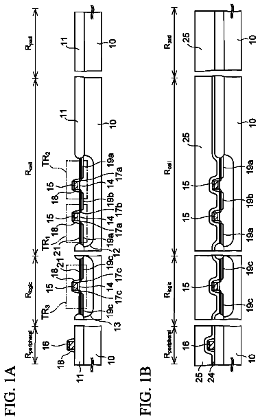
Gate height loss improvement for a transistor
The present disclosure provides a method of fabricating a semiconductor device.
US 8,598,299 B2 · Assignee: Xerox Corporation · Inventors: Wu; Yiliang et al.
Sheet 1 of 5 from the published document. All sheets in the USPTO PDF
A semiconductor composition for producing a semiconducting layer with consistently high mobility is disclosed. The semiconductor composition includes a diketopyrrolopyrrole-thiophene copolymer and a non-aromatic halogenated hydrocarbon solvent. The copolymer has a structure disclosed within. Preferably, the non-aromatic halogenated hydrocarbon solvent contains at least 2 carbon atoms and at least 3 halogen atoms.
The present disclosure relates to thin-film transistors (TFTs) and/or other electronic devices comprising a semiconducting layer. The semiconducting layer is formed from a semiconductor composition as described herein. When the composition is used in the semiconducting layer of a device, high mobility and excellent stability may be achieved. TFTs are generally composed of, on a substrate, an electrically conductive gate electrode, source and drain electrodes, an electrically insulating gate dielectric layer which separate the gate electrode from the source and drain electrodes, and a semiconducting layer which is in contact with the gate dielectric layer and bridges the source and drain electrodes. Their performance can be determined by the field effect mobility and the current on/off ratio of the overall transistor. High mobility and high on/off ratio are desired. Organic thin-film tran
All 5 drawing sheets from the published document, cropped to the drawing.
What the patent claimed, word for word. All of it is now free to use.
The present disclosure relates to thin-film transistors (TFTs) and/or other electronic devices comprising a semiconducting layer. The semiconducting layer is formed from a semiconductor composition as described herein. When the composition is used in the semiconducting layer of a device, high mobility and excellent stability may be achieved.
TFTs are generally composed of, on a substrate, an electrically conductive gate electrode, source and drain electrodes, an electrically insulating gate dielectric layer which separate the gate electrode from the source and drain electrodes, and a semiconducting layer which is in contact with the gate dielectric layer and bridges the source and drain electrodes. Their performance can be determined by the field effect mobility and the current on/off ratio of the overall transistor. High mobility and high on/off ratio are desired.
Organic thin-film transistors (OTFTs) can be used in applications such as radio frequency identification (RFID) tags and backplane switching circuits for displays, such as signage, readers, and liquid crystal displays, where high switching speeds and/or high density are not essential. They also have attractive mechanical properties such as being physically compact, lightweight, and flexible.
Organic thin-film transistors can be fabricated using low-cost solution-based patterning and deposition techniques, such as spin coating, solution casting, dip coating, stencil/screen printing, flexography, gravure, offset printing, ink jet-printing, micro-contact printing, and the like. To enable the use of these solution-based processes in fabricating thin-film transistor circuits, solution processable materials are therefore required. However, most current organic or polymeric semiconductors formed by solution processing tend to suffer from limited solubility, air sensitivity, and especially low field-effect mobility. Some poor performance, such as low field-effect mobility, may be attributable to the poor semiconductor film formed from an improper semiconductor composition.
It would be desirable to develop semiconductor compositions that can be used to form semiconducting layers that exhibit high field effect mobility, air stability, and good solubility.
The present application discloses, in various embodiments, semiconductor compositions that can be used to form semiconducting layers that have high mobility. The semiconductor compositions comprise a non-aromatic halogenated hydrocarbon solvent and a donor-acceptor type of semiconducting polymer as described herein. Desirably, the non-aromatic halogenated hydrocarbon solvent contains at least 2 carbon atoms and at least 3 halogen atoms. In some particular embodiments, the semiconducting copolymer is a copolymer comprising an optionally substituted diketopyrrolopyrrole/dithioketopyrrolopyrrole moiety and an optionally substituted thiophene moiety.
Disclosed in some embodiments is a composition comprising: a non-aromatic halogenated hydrocarbon solvent containing at least 2 carbon atoms and at least 3 halogen atoms; and a polymer of Formula (I):
##STR00001## wherein R.sub.1 and R.sub.2 are independently hydrogen, alkyl, substituted alkyl, aryl, substituted aryl, heteroaryl, or substituted heteroaryl; Y.sub.1 and Y.sub.2 are independently S or O; a is at least 1; the sum of (p+q) is at least 1; M is a conjugated moiety; b is from 0 to about 20; n is from 2 to about 5,000; and each Ar.sub.1 and Ar.sub.2 unit is independently selected from the group consisting of:
##STR00002## ##STR00003## wherein each R' is independently selected from hydrogen, alkyl, substituted alkyl, aryl, substituted aryl, heteroaryl, substituted heteroaryl, halogen, alkoxy, alkylthio, trialkylsilyl, --CN, or --NO.sub.2; and g is from 0 to 12.
In particular embodiments, the non-aromatic halogenated hydrocarbon solvent is a chloroalkane. The non-aromatic halogenated hydrocarbon solvent may be selected from the group consisting of 1,1,2,2-tetrachloroethane; 1,1,1,2-tetrachloroethane; 1,1,1,2,2-pentachloroethane; pentaerythrityl tetrachloride; 1,2,3,4-tetrachlorobutane; 1,2,3-trichloropropane; 1,1,2-trichloroethane; and 1,1,2-trichloroethylene. Desirably, the non-aromatic halogenated hydrocarbon solvent is 1,1,2,2-tetrachloroethane.
The polymer may be from about 0.01 wt % to about 5 wt % of the semiconductor composition.
In embodiments of Formula (I), R.sub.1 and R.sub.2 are alkyl. In others, Y.sub.1 and Y.sub.2 are O, or Y.sub.1 and Y.sub.2 are S. Sometimes, b is 0. Other times, the sum of (p+q) is at least 2.
In particular embodiments, the polymer has the structure of Formula (II):
##STR00004## wherein R.sub.1 and R.sub.2 are independently hydrogen, alkyl, substituted alkyl, aryl, substituted aryl, heteroaryl, or substituted heteroaryl; Y.sub.1 and Y.sub.2 are independently S or O; each X.sub.1 and X.sub.2 is independently S, Se, O, or NR'', wherein each R'' can independently be hydrogen, aryl, or alkyl; each Z.sub.1 and Z.sub.2 is independently alkyl, substituted alkyl, aryl, substituted aryl, heteroaryl, substituted heteroaryl, halogen, alkoxy, alkylthio, trialkylsilyl, --CN, or --NO.sub.2; M is a conjugated moiety; a is at least 1; b is from 0 to about 20; the sum of (c+d) is at least 1; e and f are independently from 0 to 2; and n is from 2 to about 5,000.
In other embodiments, the polymer has the structure of Formula (III):
##STR00005## wherein R.sub.1 and R.sub.2 are independently hydrogen, alkyl, substituted alkyl, aryl, substituted aryl, heteroaryl, or substituted heteroaryl; Y.sub.1 and Y.sub.2 are S or O; each Z' is independently hydrogen, alkyl, substituted alkyl, aryl, substituted aryl, heteroaryl, substituted heteroaryl, halogen, alkoxy, alkylthio, trialkylsilyl, --CN, or --NO.sub.2; and c and d are independently 1, 2, 3, or 4.
In still other embodiments, the polymer has the structure of Formula (IV):
##STR00006## wherein R.sub.1 and R.sub.2 are independently hydrogen, alkyl, substituted alkyl, aryl, substituted aryl, heteroaryl, or substituted heteroaryl; Y.sub.1 and Y.sub.2 are S or O; each Z' and R' is independently hydrogen, alkyl, substituted alkyl, aryl, substituted aryl, heteroaryl, substituted heteroaryl, halogen, alkoxy, alkylthio, trialkylsilyl, --CN, or --NO.sub.2; and c and d are independently 1 or 2.
In some different embodiments, the polymer has the structure of Formula (V):
##STR00007## wherein R.sub.1 and R.sub.2 are independently hydrogen, alkyl, substituted alkyl, aryl, substituted aryl, heteroaryl, or substituted heteroaryl; Y.sub.1 and Y.sub.2 are independently S or O; R.sub.3 and R.sub.4 are independently hydrogen, alkyl, substituted alkyl, aryl, substituted aryl, heteroaryl, substituted heteroaryl, halogen, alkoxy, alkylthio, trialkylsilyl, --CN, or --NO.sub.2; M is a conjugated moiety; a is at least 1; b is from 0 to about 20; and n is from 2 to about 5,000.
More specifically, the polymer may have the structure of one of Formulas
through (22), as discussed more thoroughly within.
The average mobility of a semiconducting layer formed from the semiconductor composition may be at least 50% greater than the average mobility of a semiconducting layer formed from a semiconductor composition containing the same polymer and a different hydrocarbon solvent containing 1 or 2 chlorine atoms, or more than 100% greater than the average mobility of a semiconducting layer formed from a semiconductor composition containing the same polymer and a different hydrocarbon solvent containing 1 or 2 chlorine atoms. Such results were unexpected from the selection of the solvent.
In some embodiments, the average mobility of a semiconducting layer formed from the semiconductor composition is at least 0.5 cm.sup.2/Vsec.
In yet other embodiments, the polymer has the structure of Formula (VI):
##STR00008## wherein R.sub.1 and R.sub.2 are independently hydrogen, alkyl, substituted alkyl, aryl, substituted aryl, heteroaryl, or substituted heteroaryl; Y.sub.1 and Y.sub.2 are independently S or O; a is at least 1; h is 0 or 1; the sum of (h+j+k) is at least 1; b is from 0 to about 20; n is from 2 to about 5,000; each Ar.sub.1 and Ar.sub.2 unit is independently selected from the group consisting of:
##STR00009## ##STR00010## wherein each R' is independently selected from hydrogen, alkyl, substituted alkyl, aryl, substituted aryl, heteroaryl, substituted heteroaryl, halogen, alkoxy, alkylthio, trialkylsilyl, --CN, or --NO.sub.2; and g is from 0 to 12; Ar.sub.3 is selected from the group consisting of
##STR00011## and M is a conjugated moiety that is not one of the possible choices for Ar.sub.1 and Ar.sub.2.
Also disclosed in embodiments is a semiconductor composition comprising: 1,1,2,2-tetrachloroethane; and a polymer selected from the group consisting of Formula (1-A), (18), (19), (20), (22), and (21-A):
##STR00012## wherein R.sub.1 and R.sub.2 are independently hydrogen, alkyl, substituted alkyl, aryl, substituted aryl, heteroaryl, or substituted heteroaryl; Y.sub.1 and Y.sub.2 are independently S or O; and R.sub.3, R.sub.4, R.sub.5, and R.sub.6 are independently hydrogen, alkyl, substituted alkyl, aryl, substituted aryl, heteroaryl, substituted heteroaryl, halogen, alkoxy, alkylthio, trialkylsilyl, --CN, or --NO.sub.2.
Still disclosed in other various embodiments is an electronic device comprising a semiconducting layer, wherein the semiconducting layer is formed from a semiconductor composition comprising: a non-aromatic halogenated hydrocarbon solvent containing at least 2 carbon atoms and at least 3 halogen atoms; and a polymer of Formula (I):
##STR00013## wherein R.sub.1 and R.sub.2 are independently hydrogen, alkyl, substituted alkyl, aryl, substituted aryl, heteroaryl, or substituted heteroaryl; Y.sub.1 and Y.sub.2 are independently S or O; a is at least 1; the sum of (p+q) is at least 1; M is a conjugated moiety; b is from 0 to about 20; n is from 2 to about 5,000; and each Ar.sub.1 and Ar.sub.2 unit is independently selected from the group consisting of:
##STR00014## ##STR00015## wherein each R' is independently selected from hydrogen, alkyl, substituted alkyl, aryl, substituted aryl, heteroaryl, substituted heteroaryl, halogen, alkoxy, alkylthio, trialkylsilyl, --CN, or --NO.sub.2; and g is from 0 to 12; wherein the average mobility of the semiconducting layer is at least 100% greater than the average mobility of a semiconducting layer formed from a semiconductor composition containing the same polymer and a different hydrocarbon solvent containing 1 or 2 chlorine atoms.
These and other non-limiting characteristics of the disclosure are more particularly disclosed below.
The following is a brief description of the drawings, which are presented for the purposes of illustrating the exemplary embodiments disclosed herein and not for the purposes of limiting the same.
FIG. 1 is a diagram of a first embodiment of a TFT according to the present disclosure.
FIG. 2 is a diagram of a second embodiment of a TFT according to the present disclosure.
FIG. 3 is a diagram of a third embodiment of a TFT according to the present disclosure.
FIG. 4 is a diagram of a fourth embodiment of a TFT according to the present disclosure.
FIG. 5 is a flow chart for an exemplary method of forming a polymer layer in accordance with the disclosure.
FIG. 6 is a flow chart illustrating an exemplary synthesis of a semiconducting polymer as disclosed herein.
FIG. 7 is a chart showing a transfer curve for a transistor in which a semiconductor composition of the present disclosure is used.
A more complete understanding of the components, processes and apparatuses disclosed herein can be obtained by reference to the accompanying drawings. These figures are merely schematic representations based on convenience and the ease of demonstrating the present disclosure, and are, therefore, not intended to indicate relative size and dimensions of the devices or components thereof and/or to define or limit the scope of the exemplary embodiments.
Although specific terms are used in the following description for the sake of clarity, these terms are intended to refer only to the particular structure of the embodiments selected for illustration in the drawings, and are not intended to define or limit the scope of the disclosure. In the drawings and the following description below, it is to be understood that like numeric designations refer to components of like function.
The modifier "about" used in connection with a quantity is inclusive of the stated value and has the meaning dictated by the context (for example, it includes at least the degree of error associated with the measurement of the particular quantity). When used in the context of a range, the modifier "about" should also be considered as disclosing the range defined by the absolute values of the two endpoints. For example, the range of "from about 2 to about 10" also discloses the range "from 2 to 10."
The term "comprising" is used herein as requiring the presence of the named component and allowing the presence of other components. The term "comprising" should be construed to include the term "consisting of", which allows the presence of only the named component, along with any impurities that might result from the manufacture of the named component.
The present disclosure relates to semiconductor compositions that can be used to form a semiconducting layer. A semiconducting layer formed from the composition is very stable in air and has high mobility. These semiconductor compositions are useful for forming layers in electronic devices, such as thin-film transistors (TFTs).
FIG. 1 illustrates a bottom-gate bottom-contact TFT configuration according to the present disclosure. The TFT 10 comprises a substrate 16 in contact with the gate electrode 18 and a gate dielectric layer 14. The gate electrode 18 is depicted here atop the substrate 16, but the gate electrode could also be located in a depression within the substrate. The gate dielectric layer 14 separates the gate electrode 18 from the source electrode 20, drain electrode 22, and the semiconducting layer 12. The semiconducting layer 12 runs over and between the source and drain electrodes 20 and 22. The semiconductor has a channel length between the source and drain electrodes 20 and 22.
FIG. 2 illustrates another bottom-gate top-contact TFT configuration according to the present disclosure. The TFT 30 comprises a substrate 36 in contact with the gate electrode 38 and a gate dielectric layer 34. The semiconducting layer 32 is placed on top of the gate dielectric layer 34 and separates it from the source and drain electrodes 40 and 42.
FIG. 3 illustrates a bottom-gate bottom-contact TFT configuration according to the present disclosure. The TFT 50 comprises a substrate 56 which also acts as the gate electrode and is in contact with a gate dielectric layer 54. The source electrode 60, drain electrode 62, and semiconducting layer 52 are located atop the gate dielectric layer 54.
FIG. 4 illustrates a top-gate top-contact TFT configuration according to the present disclosure. The TFT 70 comprises a substrate 76 in contact with the source electrode 80, drain electrode 82, and the semiconducting layer 72. The semiconducting layer 72 runs over and between the source and drain electrodes 80 and 82. The gate dielectric layer 74 is on top of the semiconducting layer 72. The gate electrode 78 is on top of the gate dielectric layer 74 and does not contact the semiconducting layer 72.
The semiconductor compositions of the present disclosure include a non-aromatic halogenated hydrocarbon solvent containing at least 2 carbon atoms and at least 3 halogen atoms; and a semiconducting polymer of Formula (I) to Formula (VI) as described herein.
The non-aromatic halogenated hydrocarbon solvent contains at least 2 carbon atoms and at least 3 halogen atoms. The phrase "non-aromatic" means that the compound used as the solvent is not aromatic. In other words, the compound does not obey Huckel's rule and does not have a delocalized conjugated pi system with a coplanar structure. The term "halogenated" means that the compound contains at least 3 halogen atoms. Halogen atoms include fluorine, chlorine, bromine, and iodine. The term "hydrocarbon" means that the solvent contains carbon atoms and hydrogen atoms, and includes alkanes, alkenes, and alkynes. In specific embodiments, the halogen atom is a chlorine atom.
In some embodiments, the non-aromatic halogenated hydrocarbon solvent contains at least 3 carbon atoms, or at least 4 carbon atoms. In some embodiments, the non-aromatic halogenated hydrocarbon solvent contains at least 4 halogen atoms, or at least 5 halogen atoms. In particular embodiments, the non-aromatic halogenated hydrocarbon solvent contains at least 2 carbon atoms and at least 4 halogen atoms. In others, the non-aromatic halogenated hydrocarbon solvent contains at least 3 carbon atoms and at least 3 halogen atoms. In still others, the non-aromatic halogenated hydrocarbon solvent contains at least 1 hydrogen atom. In particular, embodiments, the non-aromatic halogenated hydrocarbon solvent contains only carbon, hydrogen, and chlorine atoms.
In specific embodiments, the non-aromatic halogenated hydrocarbon solvent is selected from the group consisting of 1,1,2,2-tetrachloroethane (CAS #79-34-5); 1,1,1,2-tetrachloroethane (CAS #630-20-6); 1,1,1,2,2-pentachloroethane (CAS #76-01-7); pentaerythrityl tetrachloride (CAS #3228-99-7); 1,2,3,4-tetrachlorobutane (CAS #3405-32-1); 1,2,3-trichloropropane (CAS #96-18-4); 1,1,2-trichloroethane (CAS #79-00-5); and 1,1,2-trichloroethylene (CAS #79-01-6). Of course, more than one such non-aromatic halogenated hydrocarbon solvent may also be present in the semiconductor composition if desired. In other particular embodiments, the non-aromatic halogenated hydrocarbon solvent is a chloroalkane. Put another way, the only halogen present is chlorine, and the carbon atoms are all single bonds. Desirably, the non-aromatic halogenated hydrocarbon solvent is 1,1,2,2-tetrachloroethane.
Without being limited by theory, it is believed that the Hansen solubility parameters of the solvent should have a large dispersion force component (.delta..sub.D), a relatively large polar component (.delta..sub.P), and a relatively large hydrogen bonding component (.delta..sub.H). In this regard, aromatic halogenated hydrocarbon solvents usually have a low hydrogen bonding component. Table 1 lists several different solvents and their Hansen solubility parameters and boiling points. Several of these solvents are not claimed, and are only provided for reference. The components are shown in units of MPa.sup.1/2.
TABLE-US-00001 TABLE 1 # carbon # halogen bp. Solvent Aromatic? atoms atoms .delta..sub.D .delta..sub.P .delta..sub.H (.- degree. C.) Benzene Y 6 0 18.4 0.0 2.0 80.1 chlorobenzene Y 6 1 19.0 4.3 2.0 131 o-dichlorobenzene Y 6 2 19.2 6.3 3.3 180 1,2,4,5-tetrachlorobenzene Y 6 4 21.2 10.7 3.4 246 toluene Y 7 0 18.0 1.4 2.0 110.6 p-chlorotoluene Y 7 1 19.1 6.2 2.6 162 trichlorobiphenyl Y 12 3 19.2 5.3 4.1 317-336 chloromethane N 1 1 15.3 6.1 3.9 -23.7 methylene dichloride N 1 2 18.2 6.3 6.1 39 chloroform N 1 3 17.8 3.1 5.7 61.2 carbon tetrachloride N 1 4 17.8 0.0 0.6 76.7 ethyl chloride N 2 1 15.7 6.1 2.9 12.3 1,1-dichloroethane N 2 2 16.5 8.2 0.4 84 ethylene dichloride N 2 2 19.0 7.4 4.1 84 1,1-dichloroethylene N 2 2 17.0 6.8 4.5 32 1,1,1-trifluoroethane N 2 3 14.6 10.7 0.0 -47.6 1,1,1-trichloroethane N 2 3 16.8 4.3 2.0 74 trichloroethylene N 2 3 18.0 3.1 5.3 87.2 1,1,2-trichloroethane N 2 3 18.2 5.3 6.8 110-115 tetrachloroethylene N 2 4 19.0 6.5 2.9 121.1 1,1,2,2-tetrachloroethane N 2 4 18.8 5.1 9.4 146.5 1,1,2-trichlorotrifluoroethane N 2 6 14.7 1.6 0.0 47.6 1,2-dichlorotetrafluoroethane N 2 6 12.6 1.8 0.0 3.5 1-chlorobutane N 3 1 16.2 5.5 2.0 79 1,1,2,2-tetrachloropropane N 3 4 17.9 6.7 3.3 153.9 n-butane N 4 0 14.1 0.0 0.0 -0.5 cyclohexane N 6 0 16.8 0.0 0.2 80.7 cyclohexyl chloride N 6 1 17.3 5.5 2.0 142 perfluoroheptane N 7 16 12.0 0.0 0.0 82-84
As seen in Table 2, an aromatic halogenated hydrocarbon solvent such as o-dichlorobenzene has a low hydrogen bonding component of 3.3 MPa.sup.1/2, whereas the preferred non-aromatic halogenated hydrocarbon solvents have a high hydrogen bonding component, such as 1,1,2,2-tetrachloroethane which has a hydrogen bonding component of 9.4 MPa.sup.1/2. Similarly, the preferred non-aromatic halogenated hydrocarbon solvents can have a dispersion force component of at least 18.0 MPa.sup.1/2. In embodiments, the non-aromatic halogenated hydrocarbon solvent has a hydrogen bonding component .delta..sub.H of 5.0 MPa.sup.1/2 or greater. In embodiments, the non-aromatic halogenated hydrocarbon solvent has a hydrogen bonding component .delta..sub.H of at least 5.0 MPa.sup.1/2 and a dispersion force component of at least 18.0 MPa.sup.1/2. In other embodiments, the non-aromatic halogenated hydrocarbon solvent has a boiling point of at least 70.degree. C., including at least 100.degree. C. or at least 120.degree. C. Generally, the non-aromatic halogenated hydrocarbon solvent has a maximum boiling point of about 300.degree. C.
If desired, other solvents may also be present in the semiconductor composition. Such solvents may include toluene, xylene, mesitylene, ethylbenzene, diethylbenzene, trimethyl benzene, methyl ethylbenzene, tetrahydronaphthalene, chlorobenzene, dichlorobenzene, trichlorobenzene, chlorotoluene, methyl isobutyl ketone, methyl benzoate, benzyl benzoate, anisole, cyclohexanone, and acetophenone. Other solvents could be used as well, such as organoamines, methanol, ethanol, propanol, butanol, glycols, acetone, tetrahydrofuran (THF), dichloromethane, ethyl acetate, dimethylformamide (DMF), dimethyl sulfoxide (DMSO), acetic acid, acetonitrile, and dioxane. However, the amount of additional solvents (by weight) is always less than the amount of non-aromatic halogenated hydrocarbon solvent. In some particular embodiments, only non-aromatic halogenated hydrocarbon solvents are present in the semiconductor composition as a solvent.
The semiconducting polymer may have the structure of Formula (I):
##STR00016## wherein R.sub.1 and R.sub.2 are independently hydrogen, alkyl, substituted alkyl, aryl, substituted aryl, heteroaryl, or substituted heteroaryl; Y.sub.1 and Y.sub.2 are independently S or O; a is at least 1; the sum of (p+q) is at least 1; M is a conjugated moiety; b is from 0 to about 20; n is from 2 to about 5,000; and each Ar.sub.1 and Ar.sub.2 unit is independently selected from the group consisting of:
##STR00017## ##STR00018## wherein each R' is independently selected from hydrogen, alkyl, substituted alkyl, aryl, substituted aryl, heteroaryl, substituted heteroaryl, halogen, alkoxy, alkylthio, trialkylsilyl, --CN, or --NO.sub.2; and g is from 0 to 12.
The term "alkyl" refers to a radical composed entirely of carbon atoms and hydrogen atoms which is fully saturated. The alkyl radical may be linear, branched, or cyclic. The alkyl radical can be univalent or divalent, i.e. can bond to one or two different non-hydrogen atoms.
The term "aryl" refers to an aromatic radical composed entirely of carbon atoms and hydrogen atoms. When aryl is described in connection with a numerical range of carbon atoms, it should not be construed as including substituted aromatic radicals. For example, the phrase "aryl containing from 6 to 10 carbon atoms" should be construed as referring to a phenyl group (6 carbon atoms) or a naphthyl group (10 carbon atoms) only, and should not be construed as including a methylphenyl group (7 carbon atoms). The aryl radical may be univalent or divalent.
The term "heteroaryl" refers to an aromatic radical composed of carbon atoms, hydrogen atoms, and one or more heteroatoms. The carbon atoms and the heteroatoms are present in a cyclic ring or backbone of the radical. The heteroatoms are selected from O, S, and N. Exemplary heteroaryl radicals include thienyl and pyridyl.
The term "halogen" refers to fluorine, chlorine, bromine, and iodine.
The term "alkoxy" refers to an alkyl radical which is attached to an oxygen atom, i.e. --O--C.sub.nH.sub.2n+1.
The term "alkylthio" refers to an alkyl radical which is attached to a sulfur atom, i.e. --S--C.sub.nH.sub.2n+1.
The term "trialkylsilyl" refers to a radical composed of a tetravalent silicon atom having three alkyl radicals attached to the silicon atom, i.e. --Si(R).sub.3. The three alkyl radicals may be the same or different. The silicon atom attaches to the core of the compound.
The term "substituted" refers to at least one hydrogen atom on the named radical being substituted with another functional group, such as halogen, --CN, --NO.sub.2, --COOH, and --SO.sub.3H. An exemplary substituted alkyl group is a perhaloalkyl group, wherein one or more hydrogen atoms in an alkyl group are replaced with halogen atoms, such as fluorine, chlorine, iodine, and bromine. Besides the aforementioned functional groups, an alkyl group may also be substituted with an aryl or heteroaryl group. An aryl or heteroaryl group may also be substituted with alkyl or alkoxy. Exemplary substituted aryl groups include methylphenyl and methoxyphenyl. Exemplary substituted heteroaryl groups include 3-methylthienyl.
Generally, the alkyl groups independently contain from 1 to 30 carbon atoms. Similarly, the aryl groups independently contain from 6 to 30 carbon atoms. The heteroaryl groups contain from 2 to 30 carbon atoms.
Specific exemplary alkyl groups include methyl, ethyl, propyl, butyl, pentyl, hexyl, heptyl, octyl, nonyl, decyl, undecyl, dodecyl, tridecyl, tetradecyl, pentadecyl, hexadecyl, heptadecyl, octadecyl, cyclopentyl, cyclohexyl, cycloheptyl, t-butyl, isopentyl, isopropyl, 2-octyl-n-dodecyl, and isomers thereof.
Specific exemplary aryl and substituted aryl groups include phenyl, polyphenyl, and naphthyl; alkoxyphenyl groups, such as p-methoxyphenyl, m-methoxyphenyl, o-methoxyphenyl, ethoxyphenyl, p-tert-butoxyphenyl, and m-tert-butoxyphenyl; alkylphenyl groups such as 2-methylphenyl, 3-methylphenyl, 4-methylphenyl, ethylphenyl, 4-tert-butylphenyl, 4-butylphenyl, and dimethylphenyl; alkylnaphthyl groups such as methylnaphthyl and ethylnaphthyl; alkoxynaphthyl groups such as methoxynaphthyl and ethoxynaphthyl; dialkylnaphthyl groups such as dimethylnaphthyl and diethylnaphthyl; and dialkoxynaphthyl groups such as dimethoxynaphthyl and diethoxynaphthyl, other aryl groups listed as exemplary M groups, and combinations thereof.
Specific exemplary heteroaryl groups include oxazole, isoxazole, pyridine, thiazole, isothiazole, imidazole, triazole, pyrazole, furazan, thiadiazole, oxadiazole, pyridazine, pyrimidine, pyrazine, indole, isoindole, indazole, chromene, quinoline, isoquinoline, cinnoline, quinazoline, quinoxaline, naphthylidine, phthalazine, purine, pteridine, thienofuran, imidazothiazole, benzofuran, benzothiophene, benzoxazole, benzthiazole, benzthiadiazole, benzimidazole, imidazopyridine, pyrrolopyridine, pyrrolopyrimidine, pyridopyrimidine, and combinations thereof.
In some specific embodiments of Formula (I), R.sub.1 and R.sub.2 are the same. In others, R.sub.1 and R.sub.2 are both alkyl. Y.sub.1 and Y.sub.2 may be the same, i.e. both 0 or both S. In additional specific embodiments of Formula (I), b is zero. In others, the sum of (p+q) is at least 2, or is at least 4. The sum of (p+q) may be at most 20. In particular embodiments, Y.sub.1 and Y.sub.2 are O, b is 0, and the sum of (p+q) is at least 2. In still other embodiments, b may be 0 or 1.
In Formula (I), the M moiety must be different from an Ar.sub.1 or Ar.sub.2 unit, but can otherwise be chosen from the same moieties that Ar.sub.1 and Ar.sub.2 are selected from. For example, if Ar.sub.1 and Ar.sub.2 are unsubstituted thiophene, then M can be a substituted thiophene. In addition, the M moiety has a single ring structure. For example, biphenyl would be considered to be two M moieties, so M is phenyl and b=2. In particular embodiments, M is a conjugated moiety containing from about 4 to about 30 carbon atoms.
Alternatively, the semiconducting polymer may have the structure of Formula (II):
##STR00019## wherein R.sub.1 and R.sub.2 are independently hydrogen, alkyl, substituted alkyl, aryl, substituted aryl, heteroaryl, or substituted heteroaryl; Y.sub.1 and Y.sub.2 are independently S or O; each X.sub.1 and X.sub.2 is independently S, Se, O, or NR'', wherein each R'' can independently be hydrogen, aryl, or alkyl; each Z.sub.1 and Z.sub.2 is independently alkyl, substituted alkyl, aryl, substituted aryl, heteroaryl, substituted heteroaryl, halogen, alkoxy, alkylthio, trialkylsilyl, --CN, or --NO.sub.2; M is a conjugated moiety; a is at least 1; b is from 0 to about 20; the sum of (c+d) is at least 1; e and f are independently from 0 to 2; and n is from 2 to about 5,000.
In some specific embodiments of Formula (II), R.sub.1 and R.sub.2 are the same. In others, R.sub.1 and R.sub.2 are both alkyl. X.sub.1 and X.sub.2 may be the same. In others, X.sub.1 and X.sub.2 are S. Y.sub.1 and Y.sub.2 may be the same. In others, Y.sub.1 and Y.sub.2 are O. In other variants, X.sub.1 and X.sub.2 are S, and Y.sub.1 and Y.sub.2 are O. In additional specific embodiments of Formula (II), b is zero. In others, the sum of (c+d) is at least 2, or is at least 4. The sum of (c+d) may be at most 20. In particular embodiments, X.sub.1 and X.sub.2 are S, b is 0, and the sum of (c+d) is at least 2. In still other embodiments, b may be 0 or 1.
It should be noted that if a moiety in the repeating unit of the polymer of Formula (II) can be construed as corresponding to a five-membered ring containing X.sub.1/Z.sub.1 or X.sub.2/Z.sub.2, it should be so construed. In this regard, the M moiety cannot be a five-membered ring that would overlap with the rings containing X.sub.1/Z.sub.1 or X.sub.2/Z.sub.2. Put another way, M is a non-thiophene conjugated moiety. In preferred embodiments, M is a conjugated moiety containing from about 4 to about 30 carbon atoms.
Alternatively, the semiconducting polymer may have the structure of Formula (III):
##STR00020## wherein R.sub.1 and R.sub.2 are independently hydrogen, alkyl, substituted alkyl, aryl, substituted aryl, heteroaryl, or substituted heteroaryl; Y.sub.1 and Y.sub.2 are S or O; each Z' is independently hydrogen, alkyl, substituted alkyl, aryl, substituted aryl, heteroaryl, substituted heteroaryl, halogen, alkoxy, alkylthio, trialkylsilyl, --CN, or --NO.sub.2; and c and d are independently 1, 2, 3, or 4.
In some specific embodiments of Formula (III), R.sub.1 and R.sub.2 are the same. In others, R.sub.1 and R.sub.2 are both alkyl. Similarly, Z' may be selected from only hydrogen and alkyl.
Alternatively, the semiconducting polymer may have the structure of Formula (IV):
##STR00021## wherein R.sub.1 and R.sub.2 are independently hydrogen, alkyl, substituted alkyl, aryl, substituted aryl, heteroaryl, or substituted heteroaryl; Y.sub.1 and Y.sub.2 are S or O; each Z' and R' is independently hydrogen, alkyl, substituted alkyl, aryl, substituted aryl, heteroaryl, substituted heteroaryl, halogen, alkoxy, alkylthio, trialkylsilyl, --CN, or --NO.sub.2; and c and d are independently 1 or 2.
In some specific embodiments of Formula (IV), R.sub.1 and R.sub.2 are the same. In others, R.sub.1 and R.sub.2 are both alkyl. Similarly, Z' may be selected from only hydrogen and alkyl.
Alternatively, the semiconducting polymer may have the structure of Formula (V):
##STR00022## wherein R.sub.1 and R.sub.2 are independently hydrogen, alkyl, substituted alkyl, aryl, substituted aryl, heteroaryl, or substituted heteroaryl; Y.sub.1 and Y.sub.2 are independently S or O; R.sub.3 and R.sub.4 are independently hydrogen, alkyl, substituted alkyl, aryl, substituted aryl, heteroaryl, substituted heteroaryl, halogen, alkoxy, alkylthio, trialkylsilyl, --CN, or --NO.sub.2; M is a conjugated moiety; a is at least 1; b is from 0 to about 20; and n is from 2 to about 5,000.
In Formula (V), the M moiety can generally be any conjugated moiety, as with Formula (I). In particular embodiments, M is a conjugated moiety containing from about 4 to about 30 carbon atoms.
In some specific embodiments of Formula (V), R.sub.1 and R.sub.2 are the same. In others, R.sub.1 and R.sub.2 are both alkyl. Similarly, R.sub.3 and R.sub.4 are the same in some embodiments. In others, R.sub.3 and R.sub.4 are selected from only hydrogen and alkyl.
Finally, the semiconducting polymer may have the structure of Formula (VI):
##STR00023## wherein R.sub.1 and R.sub.2 are independently hydrogen, alkyl, substituted alkyl, aryl, substituted aryl, heteroaryl, or substituted heteroaryl; Y.sub.1 and Y.sub.2 are independently S or O; a is at least 1; h is 0 or 1; the sum of (h+j+k) is at least 1; b is from 0 to about 20; n is from 2 to about 5,000; each Ar.sub.1 and Ar.sub.2 unit is independently selected from the group consisting of:
##STR00024## ##STR00025## wherein each R' is independently selected from hydrogen, alkyl, substituted alkyl, aryl, substituted aryl, heteroaryl, substituted heteroaryl, halogen, alkoxy, alkylthio, trialkylsilyl, --CN, or --NO.sub.2; and g is from 0 to 12; Ar.sub.3 is selected from the group consisting of
##STR00026## and M is a conjugated moiety that is not one of the possible choices for Ar.sub.1 and Ar.sub.2.
In Formula (VI), the M moiety cannot be one of the possible choices for Ar.sub.1 and Ar.sub.2. For example, the M moiety cannot be a thiophene unit. However, the M moiety can be a thienothiophene like Ar.sub.3.
In some specific embodiments of Formula (VI), R.sub.1 and R.sub.2 are the same. In others, R.sub.1 and R.sub.2 are both alkyl. In some specific embodiments, h=1, and j and k are both 0. In other embodiments, b=0 and h=0. In others, h=1 and b=0.
It should be noted that Formulas (II), (III), (IV), (V), and (VI) are subsets of Formula (I). Similarly, Formulas (III) and (IV) are subsets of Formula (II). Also, Formulas (II), (III), (IV), and (V) are subsets of Formula (VI). The structures of Formulas (I) through (VI) are generally copolymers that include a diketopyrrolopyrrole/dithioketopyrrolopyrrole monomer or moiety. In specific embodiments, the semiconducting polymer is a copolymer comprising an optionally substituted diketopyrrolopyrrole moiety and an optionally substituted thiophene moiety. In other specific embodiments, the semiconducting polymer is a copolymer comprising an optionally substituted dithioketopyrrolopyrrole moiety and optionally substituted thiophene moiety. The structures of Formulas (II), (III), and (IV) are specific examples of such copolymers. Please note that the term "copolymer" is used herein as referring to a polymer containing two or more different monomers. The term "dipolymer" may be used to refer to a polymer containing only two different monomers, while the term "terpolymer" may be used to refer to a polymer containing only three different monomers.
Exemplary semiconducting polymers of these six formulas include those of Formulas
through (22):
##STR00027## ##STR00028## ##STR00029## ##STR00030## ##STR00031## wherein R.sub.1 and R.sub.2 are independently hydrogen, alkyl, substituted alkyl, aryl, substituted aryl, heteroaryl, or substituted heteroaryl; Y.sub.1 and Y.sub.2 are independently S or O; and each Z', R', R.sub.3, R.sub.4, R.sub.5, and R.sub.e is independently hydrogen, alkyl, substituted alkyl, aryl, substituted aryl, heteroaryl, substituted heteroaryl, halogen, alkoxy, alkylthio, trialkylsilyl, --CN, or --NO.sub.2.
Formulas (1)-
are specific examples of Formula (I). However, Formulas (1)-
and (18)-
allow b to be 0 or 1. Formula
only falls within Formula (I) when b=0.
Formulas (1)-
and (18)-
are specific examples of Formula (II). Formulas (11)-
and
only fall within Formula (II) when b=1.
Formulas (1)-
and (18)-
are specific examples of Formula (III).
Formula
is a specific example of Formula (IV). In Formula (21), c=d=1.
Formula
is a specific example of Formula (V). In Formula (22), b=2.
Formulas (1)-
are specific examples of Formula (VI). Formula
only falls within Formula (VI) when b=1. In Formulas (1)-
and (22), b=0. Formula
is an example of Formula (VI) where h=1.
In some specific embodiments of Formula (1), Y.sub.1 and Y.sub.2 are O, and R.sub.1 and R.sub.2 are alkyl. In more specific embodiments, Y.sub.1 and Y.sub.2 are O, all Z' are hydrogen, and R.sub.1 and R.sub.2 are alkyl.
In specific embodiments of Formulas (I)-(VI) and Formulas (1)-(22), R.sub.1 and R.sub.2 are the same and are alkyl. In more particular embodiments, R.sub.1 and R.sub.2 are long-chain alkyl having from about 12 to about 30 carbon atoms.
Two specific embodiments of polymers include those of Formula (1-A) and (21-A):
##STR00032## wherein R.sub.1 and R.sub.2 are independently hydrogen, alkyl, substituted alkyl, aryl, substituted aryl, heteroaryl, or substituted heteroaryl; Y.sub.1 and Y.sub.2 are independently S or O; and R.sub.3 and R.sub.4 are independently hydrogen, alkyl, substituted alkyl, aryl, substituted aryl, heteroaryl, substituted heteroaryl, halogen, alkoxy, alkylthio, trialkylsilyl, --CN, or --NO.sub.2.
Formula (1-A) corresponds to Formula
when the four Z' units are hydrogen. Similarly, Formula (21-A) corresponds to Formula
when the two Z' units are hydrogen and R.sub.3 and R.sub.4 correspond to R'.
In specific embodiments, the semiconducting polymer of Formulas (I)-(III) and (VI) is a copolymer containing a diketopyrrolopyrrole/dithioketopyrrolopyrrole monomer and a thiophene monomer. In more specific embodiments, the copolymer contains at least two thiophene monomers.
In embodiments, the semiconducting polymer of Formulas (I)-(VI) has a band gap of from about 1.1 to about 3.2 eV, including from about 1.2 to about 2.8 eV, or from about 1.2 to about 2.0 eV. In some embodiments, the semiconducting polymer of Formulas (I)-(VI) has a small band gap from about 1.0 to about 2.0 eV. This small band gap is a result of weak donor and acceptor effects of the repeating units. The diketopyrrolopyrrole unit is an electron accepting moiety, while most of the Ar.sub.1 and Ar.sub.2 moieties discussed above are electron donating moieties. This combination of electron donors and electron acceptors will result in a small band gap, yet the polymer has very good stability. The semiconducting polymer has a crystalline, semicrystalline, or liquid crystalline structure in the semiconductor layer. Crystallinity can be determined for example using X-ray diffraction method.
In specific embodiments, the semiconducting polymers are diketopyrrolopyrrole-thiophene copolymers, such as those of Formulas (1), (2), (3), (18), (19), or (20).
Exemplary polymers of the present disclosure can be prepared by a five-step process, as illustrated in FIG. 5 and FIG. 6. FIG. 6 illustrates various synthesis routes for forming a copolymer of Formula (I), where Ar.sub.1 and Ar.sub.2 are thiophene groups. The description herein discusses the formation of diketopyrrolopyrrole (DKPP) and dithioketopyrrolopyrrole (DTKPP) moieties, and the phrase DPP will be used to refer generically to either moiety.
At step S100, a DKPP (diketopyrrolopyrrole) moiety may be formed by reacting 2 moles of an appropriate nitrile or a Schiff base with one mole of a succinic acid diester in the presence of a base and an organic solvent. For example, a carbonitrile (Ar--CN) for forming the selected Ar group (e.g., thiophenecarbonitrile) is reacted with a succinate (e.g. diisopropyl succinate or di-n-butyl succinate) under suitable conditions for ring closure of the DKPP moiety to form a monomer M1 of the general formula:
##STR00033## where Ar is as defined above.
The description continues in the full USPTO document.
About 5,942 words. The USPTO PDF has it with every drawing.
Fees are due 3.5, 7.5 and 11.5 years after grant. This patent expired on December 3, 2025, so the fee marked "not paid" was the one that went unpaid.
SEMICONDUCTOR COMPOSITION
Filed Dec 2011 · published Jun 2013Semiconductor composition
Filed Dec 2011 · granted Dec 2013Earlier publications, parents and continuations. None of them can still be enforced, or this patent would not be listed.
Prior art cited by the examiner or applicant. Useful when you check your own idea for novelty.
Everything on this page comes from the documents linked above.