Patent Yard Sign in
Lapsed, fee not paid

Scanning optical apparatus and image forming apparatus using the same

US 8,594,533 B2 · Assignee: Canon Kabushiki Kaisha · Inventors: Naito; Yuuta

USPTO PDF

Overview

Sheet 1 of 17 from the published document. All sheets in the USPTO PDF

Abstract From the patent

A scanning optical apparatus includes scanning units, a deflector. Each of the apparatuses includes a light source, an imaging optical system including imaging optical elements imaging a beam deflected by the deflector on a scanning surface. The scanning surfaces are scanned with beams in opposing directions. When a main scanning direction of the first scanning unit is a Y positive direction, a sign is the same between .theta.1h(Y1min).times..theta.1r and .theta.2h(Y1min).times..theta.2r. Here, .theta.1h(y), .theta.2h(y) denote orientation angles between the Y axis and a slow axis at a Y direction position y of first/second imaging optical elements from an optical axis, the imaging optical elements each being an imaging optical element having a largest thickness among them of the imaging optical systems, .theta.1r and .theta.2r denote angles between the Y axis and polarization directions of the beams reaching the imaging optical elements, and Y1min denotes a Y position where .theta.1h(y) becomes minimum.

Why it's free to use

  • The USPTO Official Gazette of January 20, 2026 lists it as expired on November 26, 2025 for an unpaid maintenance fee.
  • It isn't on any reinstatement notice published since.
  • Its 1 US relative has also lapsed, expired or never issued.
  • We check US rights only. Check foreign counterparts before selling abroad.
FiledOctober 12, 2010
GrantedNovember 26, 2013
Expired (fee)November 26, 2025
Application number12/902582
Classification (CPC)G02B26/123 +1 more
Length18 claims · 37 pages

Background From the patent

A color image forming apparatus such as a color laser printer in recent years needs to satisfy high demands for low cost, high speed, and high image quality. As a method of realizing high speed of the color image forming apparatus, there is widely known a tandem method in which an image bearing member disposed for each color separately is scanned by a light beam so that an image for each color is formed, and later the plurality of images are superposed on a transferring medium so as to form a color image. In addition, for realizing high speed printing, a light source emitting a plurality of light beams may be used. In this case, if polarization directions of the light beams are not uniform, a ratio between P polarization component and S polarization component (polarization component ratio) for an optical element that transmits or reflects the light beams before reaching a photosensitive

Drawings 17

1 of 17 drawing sheets so far from the published document, cropped to the drawing. Every sheet is in the USPTO PDF.

Figures as described

  • FIG. 1 is a schematic diagram of a main part of a main scanning cross section according to a first embodiment of the present invention
  • FIG. 2 is a schematic diagram of a main part of a sub-scanning cross section according to the first embodiment
  • FIG. 3 is a schematic diagram of a main part of a light source unit according to the first embodiment
  • FIG. 4 is a schematic diagram illustrating an orientation angle of a molded lens according to the first embodiment
  • FIG. 5A is a graph illustrating the orientation angle of the molded lens according to the first embodiment three-dimensionally
  • FIG. 5B is a graph illustrating the orientation angle of the molded lens according to the first embodiment with a contour diagram
  • FIG. 9 is a schematic diagram illustrating an incident state of a laser deflection according to the first embodiment
  • FIG. 12A is a graph of reflectance for S and P polarized light of a turn back mirror according to the first embodiment (first turn back mirror (16a or 16b))
  • FIG. 12B is a graph of reflectance for S and P polarized light of a turn back mirror according to the first embodiment (second turn back mirror (17a for S1))
  • FIG. 12C is a graph of reflectance for S and P polarized light of a turn back mirror according to the first embodiment (second turn back mirror (17b for S2))
  • FIG. 13 is a graph showing illuminance distribution of the scanning unit S1 according to the first embodiment
  • FIG. 18 is a graph showing illuminance distribution of the scanning unit S2 according to the first embodiment

Claims 18 total, 12 independent

What the patent claimed, word for word. All of it is now free to use.

  1. 1
    Independent claimA scanning optical apparatus comprising: a first scanning unit; a second scanning unit; and a deflecting unit which deflects a light beam for scanning and is shared by the first scanning unit and the second scanning unit, the deflecting unit having a first deflecting surface and a second deflecting surface which is different from the first deflecting surface, wherein the first scanning unit includes: a first light source unit having a plurality of light-emitting points; a first incident optical system which guides a light beam emitted from the first light source unit to the first deflecting surface of the deflecting unit; and a first imaging optical system, which is disposed in an optical path of the light beam emitted from the first light source unit and deflected by the deflecting unit, including at least one imaging optical element for imaging the light beam deflected by the first deflecting surface on a first surface to be scanned, wherein the first imaging optical system includes a first imaging optical element having a largest maximum value of a thickness in an optical axis direction of the at least one imaging optical element, the first imaging optical element having a birefringence characteristic, wherein the second scanning unit includes: a second light source unit having a plurality of light-emitting points; a second incident optical system which guides a light beam emitted from the second light source unit to the second deflecting surface of the deflecting unit, to deflect the light beam from the second light source unit; and a second imaging optical system, which is disposed in an optical path of the light beam emitted from the second light source unit and deflected by the deflecting unit, including at least one imaging optical element for imaging the light beam deflected by the second deflecting surface on a second surface to be scanned, wherein the second imaging optical system includes a second imaging optical element having a largest maximum value of a thickness in an optical axis direction of the at least one imaging optical element included in the second imaging optical system, the second imaging optical element having a birefringence characteristic, wherein the light beam from the first light source unit and the light beam from the second light source unit scan the first surface to be scanned and the second surface to be scanned by rotating the deflecting unit in directions opposed to each other in a main scanning direction, and wherein the first scanning unit and the second scanning unit are configured to reduce a difference between: (a) difference between a slow axis direction of an imaging optical element included in the first imaging optical system and a polarization direction of light beam incident on the first imaging optical system from the first light source unit, and (b) a difference between a slow axis direction of an imaging optical element included in the second imaging optical system and a polarization direction of light beam incident on the second imaging optical system from the second light source unit.
  2. 2
    A scanning optical apparatus according to claim 1, wherein: the first imaging optical element and the second imaging optical element are formed by a molding process, and where a Y axis is defined as an axis which is parallel to a direction in which scanning with light beam from the first light source is performed by the deflecting unit in the first scanning unit and intersects with an optical axis of the first imaging optical element, and where a plus direction of Y axis is defined as an orientation in which scanning with a light beam from the first light source is performed by the deflecting unit in the first scanning unit and intersects with an optical axis of the first image optical element, positions of gate parts of the first imaging optical element and the second imaging optical element formed in the molding process with respect to an optical axis position are the same position in the Y axis direction and in the optical axis directions of the first imaging optical system and the second imaging optical system.
  3. 3
    Independent claimAn image forming apparatus comprising: a scanning optical apparatus; and a printer controller which converts code data supplied from an external device into an image signal, which is supplied to the scanning optical apparatus, wherein the scanning optical apparatus comprises: a first scanning unit; a second scanning unit; and a deflecting unit which deflects a light beam for scanning and is shared by the first scanning unit and the second scanning unit, the deflecting unit having a first deflecting surface and a second deflecting surface which is different from the first deflecting surface, wherein the first scanning unit includes: a first light source unit having a plurality of light-emitting points; a first incident optical system which guides a light beam emitted from the first light source unit to the first deflecting surface of the deflecting unit; and a first imaging optical system, which is disposed in an optical path of the light beam emitted from the first light source unit and deflected by the deflecting unit, including at least one imaging optical element for imaging the light beam deflected by the first deflecting surface on a first surface to be scanned, wherein the first imaging optical system includes a first imaging optical element having a largest maximum value of a thickness in an optical axis direction of the at least one imaging optical element, the first imaging optical element having a birefringence characteristic, wherein the second scanning unit includes: a second light source unit having a plurality of light-emitting points; a second incident optical system which guides a light beam emitted from the second light source unit to the second deflecting surface of the deflecting unit, to deflect the light beam from the second light source unit; and a second imaging optical system, which is disposed in an optical path of the light beam emitted from the second light source unit and deflected by the deflecting unit, including at least one imaging optical element for imaging the light beam deflected by the second deflecting surface on a second surface to be scanned, wherein the second imaging optical system includes a second imaging optical element having a largest maximum value of a thickness in an optical axis direction of the at least one imaging optical element included in the second imaging optical system, the second imaging optical element having a birefringence characteristic, wherein the light beam from the first light source unit and the light beam from the second light source unit scan the first surface to be scanned and the second surface to be scanned by rotating the deflecting unit in directions opposed to each other in a main scanning direction, and wherein the first scanning unit and the second scanning unit are configured to reduce a difference between: (a) a difference between a slow axis direction of an imaging optical element included in the first imaging optical system and a polarization direction of light beam incident on the first imaging optical system from the first light source unit, and (b) a difference between a slow axis direction of an imaging optical element included in the second imaging optical system and a polarization direction of light beam incident on the second imaging optical system from the second light source unit.
  4. 4
    Independent claimA color image forming apparatus comprising: a plurality of scanning optical apparatuses; and a plurality of image bearing members which are disposed on surfaces to be scanned of the plurality of scanning optical apparatuses so as to form images of different colors, wherein each of the scanning optical apparatuses comprises: a first scanning unit; a second scanning unit; and a deflecting unit which deflects a light beam for scanning and is shared by the first scanning unit and the second scanning unit, the deflecting unit having a first deflecting surface and a second deflecting surface which is different from the first deflecting surface, wherein the first scanning unit includes: a first light source unit having a plurality of light-emitting points; a first incident optical system which guides a light beam emitted from the first light source unit to the first deflecting surface of the deflecting unit; and a first imaging optical system, which is disposed in an optical path of the light beam emitted from the first light source unit and deflected by the deflecting unit, including at least one imaging optical element for imaging the light beam deflected by the first deflecting surface on a first surface to be scanned, wherein the first imaging optical system includes a first imaging optical element having a largest maximum value of a thickness in an optical axis direction of the at least one imaging optical element, the first imaging optical element having a birefringence characteristic, wherein the second scanning unit includes: a second light source unit having a plurality of light-emitting points; a second incident optical system which guides a light beam emitted from the second light source unit to the second deflecting surface of the deflecting unit, to deflect the light beam from the second light source unit; and a second imaging optical system, which is disposed in an optical path of the light beam emitted from the second light source unit and deflected by the deflecting unit, including at least one imaging optical element for imaging the light beam deflected by the second deflecting surface on a second surface to be scanned, wherein the second imaging optical system includes a second imaging optical element having a largest maximum value of a thickness in an optical axis direction of the at least one imaging optical element included in the second imaging optical system, the second imaging optical element having a birefringence characteristic, wherein the light beam from the first light source unit and the light beam from the second light source unit scan the first surface to be scanned and the second surface to be scanned by rotating the deflecting unit in directions opposed to each other in a main scanning direction, and wherein the first scanning unit and the second scanning unit are configured to reduce a difference between: (a) a difference between a slow axis direction of an imaging optical element included in the first imaging optical system and a polarization direction of light beam incident on the first imaging optical system from the first light source unit, and (b) a difference between a slow axis direction of an imaging optical element included in the second imaging optical system and a polarization direction of light beam incident on the second imaging optical system from the second light source unit.
  5. 5
    A color image forming apparatus according to claim 4, further comprising a printer controller which converts a color signal supplied from an external device into different color image data, which are supplied to the plurality of scanning optical apparatuses.
  6. 6
    A scanning optical apparatus according to claim 1, wherein each of the first light source unit and the second light source unit emits a laser beam.
  7. 7
    Independent claimA scanning optical apparatus comprising: a first scanning unit; a second scanning unit; and a deflecting unit which deflects a light beam for scanning and is shared by the first scanning unit and the second scanning unit, the deflecting unit having a deflecting surface, wherein the first scanning unit includes: a first light source unit having a plurality of light-emitting points; a first incident optical system which guides a light beam emitted from the first light source unit to the deflecting surface of the deflecting unit; and a first imaging optical system, which is disposed in an optical path of the light beam emitted from the first light source unit and deflected by the deflecting unit, including at least one imaging optical element for imaging the light beam deflected by the deflecting surface on a first surface to be scanned, wherein the first imaging optical system includes a first imaging optical element having a largest maximum value of a thickness in an optical axis direction of the at least one imaging optical element, the first imaging optical element having a birefringence characteristic, wherein the second scanning unit includes: a second light source unit having a plurality of light-emitting points; a second incident optical system which guides a light beam emitted from the second light source unit to the deflecting surface, to deflect the light beam from the second light source unit; and a second imaging optical system, which is disposed in an optical path of the light beam emitted from the second light source unit and deflected by the deflecting unit, including at least one imaging optical element for imaging the light beam deflected by the deflecting surface on a second surface to be scanned, wherein the second imaging optical system includes a second imaging optical element having a largest maximum value of a thickness in an optical axis direction of the at least one imaging optical element included in the second imaging optical system, the second imaging optical element having a birefringence characteristic, wherein the first incident optical system and the second incident optical system respectively guide the light beam from the first light source unit and the light beam from the second light source unit to enter the deflecting surface of the deflecting unit obliquely in a sub- scanning direction, and wherein the first scanning unit and the second scanning unit are configured to reduce a difference between: (a) difference between a slow axis direction of the first imaging optical element and a polarization direction of light beam incident on the first imaging optical system from the first light source unit, and (b) a difference between a slow axis direction of the second imaging optical element and a polarization direction of light beam incident on the second imaging optical system from the second light source unit.
  8. 8
    A scanning optical apparatus according to claim 7, wherein: the first imaging optical element and the second imaging optical element are formed by a molding process, where a Y axis is defined as an axis which is parallel to a direction in which scanning with light beam from the first light source is performed by the deflecting unit in the first scanning unit and intersects with an optical axis of the first imaging optical element, and where a plus direction of Y axis is defined as an orientation in which the scanning with light beam from the first light source is performed by the deflecting unit in the first scanning unit and intersects with an optical axis of the first imaging optical element, positions of gate parts of the first imaging optical element and the second imaging optical element formed in the molding process with respect to an optical axis position are the same position in the Y axis direction and in the optical axis directions of the first imaging optical system and the second imaging optical system.
  9. 9
    Independent claimAn image forming apparatus comprising: a scanning optical apparatus; and a printer controller which converts code data supplied from an external device into an image signal, which is supplied to the scanning optical apparatus, wherein the scanning optical apparatus comprises: a first scanning unit; a second scanning unit; and a deflecting unit which deflects a light beam for scanning and is shared by the first scanning unit and the second scanning unit, the deflecting unit having a deflecting surface, wherein the first scanning unit includes: a first light source unit having a plurality of light-emitting points; a first incident optical system which guides a light beam emitted from the first light source unit to the deflecting surface of the deflecting unit; and a first imaging optical system, which is disposed in an optical path of the light beam emitted from the first light source unit and deflected by the deflecting unit, including at least one imaging optical element for imaging the light beam deflected by the deflecting surface on a first surface to be scanned, wherein the first imaging optical system includes a first imaging optical element having a largest maximum value of a thickness in an optical axis direction of the at least one imaging optical element, the first imaging optical element having a birefringence characteristic, wherein the second scanning unit includes: a second light source unit having a plurality of light-emitting points; a second incident optical system which guides a light beam emitted from the second light source unit to the deflecting surface of the deflecting unit; and a second imaging optical system, which is disposed in an optical path of the light beam emitted from the second light source unit and deflected by the deflecting unit, including at least one imaging optical element for imaging the light beam deflected by the deflecting surface on a second surface to be scanned, wherein the second imaging optical system includes a second imaging optical element having a largest maximum value of a thickness in an optical axis direction of the at least one imaging optical element included in the second imaging optical system, the second imaging optical element having a birefringence characteristic, wherein the light beam from the first light source unit and the light beam from the second light source unit scan the first surface to be scanned and the second surface to be scanned by rotating the deflecting unit in directions opposed to each other in a main scanning direction, and wherein the first scanning unit and the second scanning unit are configured to reduce a difference between: (a) difference between a slow axis direction of the first imaging optical element and a polarization direction of light beam incident on the first imaging optical system from the first light source unit, and (b) a difference between a slow axis direction of the second imaging optical element and a polarization direction of light beam incident on the second imaging optical system from the second light source unit.
  10. 10
    Independent claimA color image forming apparatus comprising: a plurality of scanning optical apparatuses each comprising the scanning optical apparatus; and a plurality of image bearing members which are disposed on surfaces to be scanned of the plurality of scanning optical apparatuses so as to form images of different colors, wherein the scanning optical apparatus comprises: a first scanning unit; a second scanning unit; and a deflecting unit which deflects a light beam for scanning and is shared by the first scanning unit and the second scanning unit, the deflecting unit having a first deflecting surface and a second deflecting surface which is different from the first deflecting surface, wherein the first scanning unit includes: a first light source unit having a plurality of light-emitting points; a first incident optical system which guides a light beam emitted from the first light source unit to the deflecting surface of the deflecting unit; and a first imaging optical system, which is disposed in an optical path of the light beam emitted from the first light source unit and deflected by the deflecting unit, including at least one imaging optical element for imaging the light beam deflected by the deflecting surface on a first surface to be scanned, wherein the first imaging optical system includes a first imaging optical element having a largest maximum value of a thickness in an optical axis direction of the at least one imaging optical element, the first imaging optical element having a birefringence characteristic, wherein the second scanning unit includes: a second light source unit having a plurality of light-emitting points; a second incident optical system which guides a light beam emitted from the second light source unit to the deflecting surface of the deflecting unit; and a second imaging optical system, which is disposed in an optical path of the light beam emitted from the second light source unit and deflected by the deflecting unit, including at least one imaging optical element for imaging the light beam deflected by the deflecting surface on a second surface to be scanned, wherein the second imaging optical system includes a second imaging optical element having a largest maximum value of a thickness in an optical axis direction of the at least one imaging optical element included in the second imaging optical system, the second imaging optical element having a birefringence characteristic, wherein the light beam from the first light source unit and the light beam from the second light source unit scan the first surface to be scanned and the second surface to be scanned by rotating the deflecting unit in directions opposed to each other in a main scanning direction, and wherein the first scanning unit and the second scanning unit are configured to reduce a difference between: (a) difference between a slow axis direction of the first imaging optical element and a polarization direction of light beam incident on the first imaging optical system from the first light source unit, and (b) a difference between a slow axis direction of the second imaging optical element and a polarization direction of light beam incident on the second imaging optical system from the second light source unit.
  11. 11
    A color image forming apparatus according to claim 10, further comprising a printer controller which converts a color signal supplied from an external device into different color image data, which are supplied to the plurality of scanning optical apparatuses.
  12. 12
    A scanning optical apparatus according to claim 7, wherein each of the first light source unit and the second light source unit emits a laser beam.
  13. 13
    Independent claimA scanning optical apparatus comprising: a first scanning unit; a second scanning unit; and a deflecting unit which deflects a light beam for scanning and is shared by the first scanning unit and the second scanning unit, the deflecting unit having a first deflecting surface and a second deflecting surface which is different from the first deflecting surface, wherein the first scanning unit includes: a first light source unit having a plurality of light-emitting points; a first incident optical system which guides a light beam emitted from the first light source unit to the first deflecting surface of the deflecting unit; and a first imaging optical system, which is disposed in an optical path of the light beam emitted from the first light source unit and deflected by the deflecting unit, including at least one imaging optical element for imaging the light beam deflected by the first deflecting surface on a first surface to be scanned, wherein the first imaging optical system includes a first imaging optical element having a largest maximum value of a thickness in an optical axis direction of the at least one imaging optical element, the first imaging optical element having a birefringence characteristic, wherein the second scanning unit includes: a second light source unit having a plurality of light-emitting points; a second incident optical system which guides a light beam emitted from the second light source unit to the second deflecting surface of the deflecting unit, to deflect the light beam from the second light source unit; and a second imaging optical system, which is disposed in an optical path of the light beam emitted from the second light source unit and deflected by the deflecting unit, including at least one imaging optical element for imaging the light beam deflected by the second deflecting surface on a second surface to be scanned, wherein the second imaging optical system includes a second imaging optical element having a largest maximum value of a thickness in an optical axis direction of the at least one imaging optical element included in the second imaging optical system, the second imaging optical element having a birefringence characteristic, wherein the light beam from the first light source unit and the light beam from the second light source unit scan the first surface to be scanned and the second surface to be scanned by rotating the deflecting unit in directions opposed to each other in a main scanning direction, and wherein the following expressions are satisfied: Y1min.times..theta.2r>0, in a case where Y1min.times..theta.1r>0 is satisfied; and Y1min.times..theta.2r<0, in a case where Y1min.times..theta.1r<0 is satisfied, where a direction in which the first surface to be scanned is scanned with the light beam from the first light source unit in the main scanning direction is defined as a positive direction of a Y axis, .theta.1h(y) and .theta.2h(y) respectively denote orientation angles that are angles between the main scanning direction and a slow axis direction at a position y in the Y axis direction when an intersection between the Y axis and a plane perpendicular to the Y axis including the optical axis is regarded as an origin of the Y axis in the first imaging optical element and the second imaging optical element, .theta.1r and .theta.2r respectively denote angles between the Y axis and polarization directions of the light beams reaching the first imaging optical element and the second imaging optical element, and Yl min denotes a position in the Y axis direction at which the orientation angle .theta.1h(y) becomes minimum.
  14. 14
    Independent claimAn image forming apparatus comprising: a scanning optical apparatus; and a printer controller which converts code data supplied from an external device into an image signal, which is supplied to the scanning optical apparatus, wherein the scanning optical apparatus comprises: a first scanning unit; a second scanning unit; and a deflecting unit which deflects a light beam for scanning and is shared by the first scanning unit and the second scanning unit, the deflecting unit having a first deflecting surface and a second deflecting surface which is different from the first deflecting surface, wherein the first scanning unit includes: a first light source unit having a plurality of light-emitting points; a first incident optical system which guides a light beam emitted from the first light source unit to the first deflecting surface of the deflecting unit; and a first imaging optical system, which is disposed in an optical path of the light beam emitted from the first light source unit and deflected by the deflecting unit, including at least one imaging optical element for imaging the light beam deflected by the first deflecting surface on a first surface to be scanned, wherein the first imaging optical system includes a first imaging optical element having a largest maximum value of a thickness in an optical axis direction of the at least one imaging optical element, the first imaging optical element having a birefringence characteristic, wherein the second scanning unit includes: a second light source unit having a plurality of light-emitting points; a second incident optical system which guides a light beam emitted from the second light source unit to the second deflecting surface of the deflecting unit, to deflect the light beam from the second light source unit; and a second imaging optical system, which is disposed in an optical path of the light beam emitted from the second light source unit and deflected by the deflecting unit, including at least one imaging optical element for imaging the light beam deflected by the second deflecting surface on a second surface to be scanned, wherein the second imaging optical system includes a second imaging optical element having a largest maximum value of a thickness in an optical axis direction of the at least one imaging optical element included in the second imaging optical system, the second imaging optical element having a birefringence characteristic, wherein the light beam from the first light source unit and the light beam from the second light source unit scan the first surface to be scanned and the second surface to be scanned by rotating the deflecting unit in directions opposed to each other in a main scanning direction, and wherein the following expressions are satisfied: Y1min.times..theta.2r>0, in a case where Y1min.times..theta.1r>0 is satisfied; and Y1min.times..theta.2r<0, in a case where Y1min.times..theta.1r<0 is satisfied, where a direction in which the first surface to be scanned is scanned with the light beam from the first light source unit in the main scanning direction is defined as a positive direction of a Y axis, .theta.1h(y) and .theta.2h(y) respectively denote orientation angles that are angles between the main scanning direction and a slow axis direction at a position y in the Y axis direction when an intersection between the Y axis and a plane perpendicular to the Y axis including the optical axis is regarded as an origin of the Y axis in the first imaging optical element and the second imaging optical element, .theta.1r and .theta.2r respectively denote angles between the Y axis and polarization directions of the light beams reaching the first imaging optical element and the second imaging optical element, and Y1 min denotes a position in the Y axis direction at which the orientation angle .theta.1h(y) becomes minimum.
  15. 15
    Independent claimA color image forming apparatus comprising: a plurality of scanning optical apparatuses each comprising the scanning optical apparatus; and a plurality of image bearing members which are disposed on surfaces to be scanned of the plurality of scanning optical apparatuses so as to form images of different colors, wherein the scanning optical apparatus comprises: a first scanning unit; a second scanning unit; and a deflecting unit which deflects a light beam for scanning and is shared by the first scanning unit and the second scanning unit, the deflecting unit having a first deflecting surface and a second deflecting surface which is different from the first deflecting surface, wherein the first scanning unit includes: a first light source unit having a plurality of light-emitting points; a first incident optical system which guides a light beam emitted from the first light source unit to the first deflecting surface of the deflecting unit; and a first imaging optical system, which is disposed in an optical path of the light beam emitted from the first light source unit and deflected by the deflecting unit, including at least one imaging optical element for imaging the light beam deflected by the first deflecting surface on a first surface to be scanned, wherein the first imaging optical system includes a first imaging optical element having a largest maximum value of a thickness in an optical axis direction of the at least one imaging optical element, the first imaging optical element having a birefringence characteristic, wherein the second scanning unit includes: a second light source unit having a plurality of light-emitting points; a second incident optical system which guides a light beam emitted from the second light source unit to the second deflecting surface of the deflecting unit, to deflect the light beam from the second light source unit; and a second imaging optical system, which is disposed in an optical path of the light beam emitted from the second light source unit and deflected by the deflecting unit, including at least one imaging optical element for imaging the light beam deflected by the second deflecting surface on a second surface to be scanned, wherein the second imaging optical system includes a second imaging optical element having a largest maximum value of a thickness in an optical axis direction of the at least one imaging optical element included in the second imaging optical system, the second imaging optical element having a birefringence characteristic, wherein the light beam from the first light source unit and the light beam from the second light source unit scan the first surface to be scanned and the second surface to be scanned by rotating the deflecting unit in directions opposed to each other in a main scanning direction, and wherein the following expressions are satisfied: Y1min.times..theta.2r>0, in a case where Y1min.times..theta.1r>0 is satisfied; and Y1min.times..theta.2r<0, in a case where Y1min.times..theta.1r<0 is satisfied, where a direction in which the first surface to be scanned is scanned with the light beam from the first light source unit in the main scanning direction is defined as a positive direction of a Y axis, .theta.1h(y) and .theta.2h(y) respectively denote orientation angles that are angles between the main scanning direction and a slow axis direction at a position y in the Y axis direction when an intersection between the Y axis and a plane perpendicular to the Y axis including the optical axis is regarded as an origin of the Y axis in the first imaging optical element and the second imaging optical element, .theta.1r and .theta.2r respectively denote angles between the Y axis and polarization directions of the light beams reaching the first imaging optical element and the second imaging optical element, and Y1 min denotes a position in the Y axis direction at which the orientation angle .theta.1h(y) becomes minimum.
  16. 16
    Independent claimA scanning optical apparatus comprising: a first scanning unit; a second scanning unit; and a deflecting unit which deflects a light beam for scanning and is shared by the first scanning unit and the second scanning unit, the deflecting unit having a deflecting surface, wherein the first scanning unit includes: a first light source unit having a plurality of light-emitting points; a first incident optical system which guides a light beam emitted from the first light source unit to the deflecting surface of the deflecting unit; and a first imaging optical system, which is disposed in an optical path of the light beam emitted from the first light source unit and deflected by the deflecting unit, including at least one imaging optical element for imaging the light beam deflected by the deflecting surface on a first surface to be scanned, wherein the first imaging optical system includes a first imaging optical element having a largest maximum value of a thickness in an optical axis direction of the at least one imaging optical element, the first imaging optical element having a birefringence characteristic, wherein the second scanning unit includes: a second light source unit having a plurality of light-emitting points; a second incident optical system which guides a light beam emitted from the second light source unit to the deflecting surface, to deflect the light beam from the second light source unit; and a second imaging optical system, which is disposed in an optical path of the light beam emitted from the second light source unit and deflected by the deflecting unit, including at least one imaging optical element for imaging the light beam deflected by the deflecting surface on a second surface to be scanned, wherein the second imaging optical system includes a second imaging optical element having a largest maximum value of a thickness in an optical axis direction of the at least one imaging optical element included in the second imaging optical system, the second imaging optical element having a birefringence characteristic, wherein the first incident optical system and the second incident optical system respectively guide the light beam from the first light source unit and the light beam from the second light source unit to enter the deflecting surface of the deflecting unit obliquely in a sub- scanning direction, and wherein the following expressions are satisfied: Y1min.times..theta.2r>0, in a case where Y1min.times..theta.1r>0 is satisfied; and Y1min.times..theta.2r<0, in a case where Y1min.times..theta.1r<0 is satisfied, where a direction in which the first surface to be scanned is scanned with the light beam from the first light source unit in the main scanning direction is defined as a positive direction of a Y axis, .theta.1h(y) and .theta.2h(y) respectively denote orientation angles that are angles between the main scanning direction and a slow axis direction at a position y in the Y axis direction when an intersection between the Y axis and a plane perpendicular to the Y axis including the optical axis is regarded as an origin of the Y axis in the first imaging optical element and the second imaging optical element, .theta.1r and .theta.2r respectively denote angles between the Y axis and polarization directions of the light beams reaching the first imaging optical element and the second imaging optical element, and Y1min denotes a position in the Y axis direction at which the orientation angle .theta.1h(y) becomes minimum.
  17. 17
    Independent claimAn image forming apparatus comprising: a scanning optical apparatus; and a printer controller which converts code data supplied from an external device into an image signal, which is supplied to the scanning optical apparatus, wherein the scanning optical apparatus comprises: a first scanning unit; a second scanning unit; and a deflecting unit which deflects a light beam for scanning and is shared by the first scanning unit and the second scanning unit, the deflecting unit having a deflecting surface, wherein the first scanning unit includes: a first light source unit having a plurality of light-emitting points; a first incident optical system which guides a light beam emitted from the first light source unit to the deflecting surface of the deflecting unit; and a first imaging optical system, which is disposed in an optical path of the light beam emitted from the first light source unit and deflected by the deflecting unit, including at least one imaging optical element for imaging the light beam deflected by the deflecting surface on a first surface to be scanned, wherein the first imaging optical system includes a first imaging optical element having a largest maximum value of a thickness in an optical axis direction of the at least one imaging optical element, the first imaging optical element having a birefringence characteristic, wherein the second scanning unit includes: a second light source unit having a plurality of light-emitting points; a second incident optical system which guides a light beam emitted from the second light source unit to the deflecting surface of the deflecting unit, to deflect the light beam from the first light source unit; and a second imaging optical system, which is disposed in an optical path of the light beam emitted from the second light source unit and deflected by the deflecting unit, including at least one imaging optical element for imaging the light beam deflected by the deflecting surface on a second surface to be scanned, wherein the second imaging optical system includes a second imaging optical element having a largest maximum value of a thickness in an optical axis direction of the at least one imaging optical element included in the second imaging optical system, the second imaging optical element having a birefringence characteristic, wherein the light beam from the first light source unit and the light beam from the second light source unit scan the first surface to be scanned and the second surface to be scanned by rotating the deflecting unit in directions opposed to each other in a main scanning direction, and wherein the following expressions are satisfied: Y1min.times..theta.2r>0, in a case where Y1min.times..theta.1r>0 is satisfied; and Y1min.times..theta.2r<0 in a case where Y1min.times..theta.1r<0 is satisfied, where a direction in which the first surface to be scanned is scanned with the light beam from the first light source unit in the main scanning direction is defined as a positive direction of a Y axis, .theta.1h(y) and .theta.2h(y) respectively denote orientation angles that are angles between the main scanning direction and a slow axis direction at a position y in the Y axis direction when an intersection between the Y axis and a plane perpendicular to the Y axis including the optical axis is regarded as an origin of the Y axis in the first imaging optical element and the second imaging optical element, .theta.1r and .theta.2r respectively denote angles between the Y axis and polarization directions of the light beams reaching the first imaging optical element and the second imaging optical element, and Y1 min denotes a position in the Y axis direction at which the orientation angle .theta.1h(y) becomes minimum.
  18. 18
    Independent claimA color image forming apparatus comprising: a plurality of scanning optical apparatuses each comprising the scanning optical apparatus; and a plurality of image bearing members which are disposed on surfaces to be scanned of the plurality of scanning optical apparatuses so as to form images of different colors, wherein the scanning optical apparatus comprises: a first scanning unit; a second scanning unit; and a deflecting unit which deflects a light beam for scanning and is shared by the first scanning unit and the second scanning unit, the deflecting unit having a deflecting surface, wherein the first scanning unit includes: a first light source unit having a plurality of light-emitting points; a first incident optical system which guides a light beam emitted from the first light source unit to the deflecting surface of the deflecting unit; and a first imaging optical system, which is disposed in an optical path of the light beam emitted from the first light source unit and deflected by the deflecting unit, including at least one imaging optical element for imaging the light beam deflected by the first deflecting surface on a first surface to be scanned, wherein the first imaging optical system includes a first imaging optical element having a largest maximum value of a thickness in an optical axis direction of the at least one imaging optical element, the first imaging optical element having a birefringence characteristic, wherein the second scanning unit includes: a second light source unit having a plurality of light-emitting points; a second incident optical system which guides a light beam emitted from the second light source unit to the deflecting surface of the deflecting unit, to deflect the light beam from the first light source unit; and a second imaging optical system, which is disposed in an optical path of the light beam emitted from the second light source unit and deflected by the deflecting unit, including at least one imaging optical element for imaging the light beam deflected by the deflecting surface on a second surface to be scanned, wherein the second imaging optical system includes a second imaging optical element having a largest maximum value of a thickness in an optical axis direction of the at least one imaging optical element included in the second imaging optical system, the second imaging optical element having a birefringence characteristic, wherein the light beam from the first light source unit and the light beam from the second light source unit scan the first surface to be scanned and the second surface to be scanned by rotating the deflecting unit in directions opposed to each other in a main scanning direction, and wherein the following expressions are satisfied: Y1min.times..theta.2r>0, in a case where Y1min.times..theta.1r>0 is satisfied; and Y1min.times..theta.2r<0, in a case where Y1min.times..theta.1r<0 is satisfied, where a direction in which the first surface to be scanned is scanned with the light beam from the first light source unit in the main scanning direction is defined as a positive direction of a Y axis, .theta.1h(y) and .theta.2h(y) respectively denote orientation angles that are angles between the main scanning direction and a slow axis direction at a position y in the Y axis direction when an intersection between the Y axis and a plane perpendicular to the Y axis including the optical axis is regarded as an origin of the Y axis in the first imaging optical element and the second imaging optical element, .theta.1r and .theta.2r respectively denote angles between the Y axis and polarization directions of the light beams reaching the first imaging optical element and the second imaging optical element, and Yl min denotes a position in the Y axis direction at which the orientation angle .theta.1h(y) becomes minimum.

Claim map

Independent claims stand on their own. The others add detail to the claim they name.

Claim 12 claims build on it
Claim 3No claims build on it
Claim 41 claim builds on it
Claim 72 claims build on it
Claim 9No claims build on it
Claim 101 claim builds on it
Claim 13No claims build on it
Claim 14No claims build on it
Claim 15No claims build on it
Claim 16No claims build on it
Claim 17No claims build on it
Claim 18No claims build on it

Description

Background of the invention

1. Field of the invention

The present invention relates to a scanning optical apparatus and an image forming apparatus using the same, which are suitable for an image forming apparatus using an electrophotography process such as a color laser beam printer, a color digital copying machine, or a color multifunction printer.

2. Description of the related art

A color image forming apparatus such as a color laser printer in recent years needs to satisfy high demands for low cost, high speed, and high image quality. As a method of realizing high speed of the color image forming apparatus, there is widely known a tandem method in which an image bearing member disposed for each color separately is scanned by a light beam so that an image for each color is formed, and later the plurality of images are superposed on a transferring medium so as to form a color image.

In addition, for realizing high speed printing, a light source emitting a plurality of light beams may be used. In this case, if polarization directions of the light beams are not uniform, a ratio between P polarization component and S polarization component (polarization component ratio) for an optical element that transmits or reflects the light beams before reaching a photosensitive member as the image bearing member is different among the light beams. As a result, a light amount at each image height on a surface to be scanned (illuminance distribution) is different among the light beams.

In order to solve this problem, there is known a scanning optical apparatus in which P polarization reflectance and S polarization reflectance are set to be substantially the same for the optical element that transmits or reflects the light beams. Thus, even in the case where the polarization component ratio changes from a design value, unevenness in illuminance distribution on the surface to be scanned is decreased.

For instance, Japanese Patent Application Laid-Open No. H11-326807 discloses an example in which a linear polarization direction of a laser is adjusted for correcting shading (illuminance distribution) on an image bearing member. Japanese Patent Application Laid-Open No. 2001-337285 discloses an example in which reflectances for S-polarized and P-polarized lights are set to be substantially the same as each other so that an illuminance distribution becomes uniform.

However, in the conventional technology described above in Japanese Patent Application Laid-Open No. H11-326807, it is necessary to adjust the polarization direction of each of the lasers while checking the illuminance distribution to correct the illuminance distribution. Therefore, as the number of light sources increases, assembly cost in the adjustment increases. In addition, in the conventional technology described above in Japanese Patent Application Laid-Open No. 2001-337285, it is difficult to set exactly the same reflectance for the P-polarized light and for the S-polarized light.

Summary of the invention

Therefore, an object of the present invention is to provide a scanning optical apparatus that can make the illuminance distribution uniform between optical paths without adjustment and with a simple structure, and an image forming apparatus including the scanning optical apparatus.

According to a first aspect of the present invention, there is provided a scanning optical apparatus, including; a first scanning unit, a second scanning unit, and a deflecting unit which deflects a light beam for scanning and is shared by the first scanning unit and the second scanning unit, in which; the first scanning unit includes a first light source unit, a first incident optical system which guides a light beam emitted from the first light source unit to a first deflecting surface of the deflecting unit, and a first imaging optical system which is disposed in an optical path of the light beam emitted from the first light source unit and deflected by the deflecting unit and includes at least one imaging optical element for imaging the light beam deflected by the first deflecting surface on a first surface to be scanned, the second scanning unit includes a second light source unit, a second incident optical system which guides a light beam emitted from the second light source unit to a second deflecting surface of the deflecting unit, which is different from the first deflecting surface for deflecting the light beam from the first light source unit, and a second imaging optical system which is disposed in an optical path of the light beam emitted from the second light source unit and deflected by the deflecting unit and includes at least one imaging optical element for imaging the light beam deflected by the second deflecting surface on a second surface to be scanned, the light beam from the first light source unit and the light beam from the second light source unit scan the first surface to be scanned and the second surface to be scanned by the rotation of the deflecting unit in directions opposed to each other in a main scanning direction, and when an imaging optical element having a largest maximum value of a thickness in an optical axis direction of the at least one imaging optical element included in the first imaging optical system is defined as a first imaging optical element, an imaging optical element having a largest maximum value of a thickness in an optical axis direction of the at least one imaging optical element included in the second imaging optical system is defined as a second imaging optical element, and a direction in which the first surface to be scanned is scanned with the light beam from the first light source unit in the main scanning direction is defined as a positive direction of a Y axis, the following expressions are satisfied; .theta.2h(Y1min).times..theta.2r>0, in a case where .theta.1h(Y1min).times..theta.1r>0 is satisfied, and .theta.2h(Y1min).times..theta.2r<0, in a case where .theta.1h(Y1min).times..theta.1r<0 is satisfied, where .theta.1h(y) and .theta.2h(y) respectively denote orientation angles that are angles between the main scanning direction and a slow axis direction at a position y in the Y axis direction when a position of the optical axis is regarded as an origin of the Y axis in the first imaging optical element and the second imaging optical element, .theta.1r and .theta.2r respectively denote angles between the Y axis and polarization directions of the light beams reaching the first imaging optical element and the second imaging optical element, and Y1min denotes a position in the Y axis direction at which the orientation angle .theta.1h(y) becomes minimum.

According to a second aspect of the present invention, there is provided a scanning optical apparatus, including; a first scanning unit, a second scanning unit; and a deflecting unit which deflects a light beam for scanning and is shared by the first scanning unit and the second scanning unit, in which; the first scanning unit includes a first light source unit, a first incident optical system which guides a light beam emitted from the first light source unit to a deflecting surface of the deflecting unit, and a first imaging optical system which is disposed in an optical path of the light beam emitted from the first light source unit and deflected by the deflecting unit and includes at least one imaging optical element for imaging the light beam deflected by the deflecting surface on a first surface to be scanned, the second scanning unit includes a second light source unit, a second incident optical system which guides a light beam emitted from the second light source unit to the deflecting surface for deflecting the light beam from the first light source unit, and a second imaging optical system which is disposed in an optical path of the light beam emitted from the second light source unit and deflected by the deflecting unit and includes at least one imaging optical element for imaging the light beam deflected by the deflecting surface on a second surface to be scanned, the first incident optical system and the second incident optical system respectively guide the light beam from the first light source unit and the light beam from the second light source unit to enter the deflecting surface of the deflecting unit obliquely in a sub-scanning direction, and when an imaging optical element having a largest maximum value of a thickness in an optical axis direction of the at least one imaging optical element included in the first imaging optical system is defined as a first imaging optical element, an imaging optical element having a largest maximum value of a thickness in an optical axis direction of the at least one imaging optical element included in the second imaging optical system is defined as a second imaging optical element, an orientation angle defined as an angle between a slow axis direction and a main scanning direction in the first imaging optical element and the second imaging optical element has a difference of 15 degrees or larger between a maximum value and a minimum value in the main scanning direction, and a direction in which the first surface to be scanned is scanned with the light beam from the first light source unit in the main scanning direction is defined as a positive direction of a Y axis, the following expressions are satisfied; .theta.2h(Y1min).times..theta.2r>0, in a case where .theta.1h(Y1min).times..theta.1r>0 is satisfied, and .theta.2h(Y1min).times..theta.2r<0, in a case where .theta.1h(Y1min).times..theta.1r<0 is satisfied, where .theta.1h(y) and .theta.2h(y) respectively denote orientation angles at a position y in the Y axis direction when a position of the optical axis is regarded as an origin of the Y axis in the first imaging optical element and the second imaging optical element, .theta.1r and .theta.2r respectively denote angles between the Y axis and polarization directions of the light beams reaching the first imaging optical element and the second imaging optical element, and Y1min denotes a position in the Y axis direction at which the orientation angle .theta.1h(y) becomes minimum.

According to the present invention, it is possible to provide the scanning optical apparatus and the image forming apparatus having little unevenness of the illuminance distribution among a plurality of optical paths so that a high quality image can be formed.

Further features of the present invention will become apparent from the following description of exemplary embodiments with reference to the attached drawings.

Brief description of the drawings

FIG. 1 is a schematic diagram of a main part of a main scanning cross section according to a first embodiment of the present invention.

FIG. 2 is a schematic diagram of a main part of a sub-scanning cross section according to the first embodiment.

FIG. 3 is a schematic diagram of a main part of a light source unit according to the first embodiment.

FIG. 4 is a schematic diagram illustrating an orientation angle of a molded lens according to the first embodiment.

FIG. 5A is a graph illustrating the orientation angle of the molded lens according to the first embodiment three-dimensionally.

FIG. 5B is a graph illustrating the orientation angle of the molded lens according to the first embodiment with a contour diagram.

FIG. 6 is a graph of an orientation angle .theta.h of a scanning unit S1 according to the first embodiment.

FIG. 7A is a schematic diagram illustrating a laser polarization direction of the scanning unit S1 according to the first embodiment (in the case of being parallel to the main scanning direction).

FIG. 7B is a schematic diagram illustrating a laser polarization direction of the scanning unit S1 according to the first embodiment (in the case of being inclined to the main scanning direction).

FIG. 8 is a graph of a laser polarization angle .theta.r' of the scanning unit S1 according to the first embodiment.

FIG. 9 is a schematic diagram illustrating an incident state of a laser deflection according to the first embodiment.

FIG. 10 is a graph of (.theta.h-.theta.r') of the scanning unit S1 according to the first embodiment.

FIG. 11 is a graph of .theta.h and .theta.r' of the scanning unit S1 according to the first embodiment.

FIG. 12A is a graph of reflectance for S and P polarized light of a turn back mirror according to the first embodiment (first turn back mirror (16a or 16b)).

FIG. 12B is a graph of reflectance for S and P polarized light of a turn back mirror according to the first embodiment (second turn back mirror (17a for S1)).

FIG. 12C is a graph of reflectance for S and P polarized light of a turn back mirror according to the first embodiment (second turn back mirror (17b for S2)).

FIG. 13 is a graph showing illuminance distribution of the scanning unit S1 according to the first embodiment.

FIG. 14 is a graph of the orientation angle .theta.h of a scanning unit S2 according to the first embodiment.

FIG. 15 is a graph of .theta.h and .theta.r' in the case where a laser rotation angle of the scanning unit S2 is -3.92 degrees in the device structure of the first embodiment.

FIG. 16 is a graph showing illuminance distribution in the case where a laser rotation angle of the scanning unit S2 is -3.92 degrees in the device structure of the first embodiment.

FIG. 17 is a graph of .theta.h and .theta.r' of the scanning unit S2 according to the first embodiment.

FIG. 18 is a graph showing illuminance distribution of the scanning unit S2 according to the first embodiment.

FIG. 19 is a schematic diagram of a main part of a main scanning cross section according to a second embodiment of the present invention.

FIG. 20 is a schematic diagram of a main part of a sub-scanning cross section according to the second embodiment.

FIG. 21A is a graph of reflectance for S and P polarized light of a turn back mirror according to the second embodiment (first turn back mirror (16a)).

FIG. 21B is a graph of reflectance for S and P polarized light of a turn back mirror according to the second embodiment (first turn back mirror (16b)).

FIG. 21C is a graph of reflectance for S and P polarized light of a turn back mirror according to the second embodiment (second turn back mirror (17b)).

FIG. 22 is a graph of .theta.h and .theta.r' of a scanning unit S1 according to the second embodiment.

FIG. 23 is a graph showing illuminance distribution of the scanning unit S1 according to the second embodiment.

FIG. 24 is a graph of .theta.h and .theta.r' in the case where a laser rotation angle of a scanning unit S2 is 5.51 degrees in the device structure of the second embodiment.

FIG. 25 is a graph showing illuminance distribution in the case where a laser rotation angle of the scanning unit S2 is 5.51 degrees in the device structure of the second embodiment.

FIG. 26 is a graph of .theta.h and .theta.r' of the scanning unit S2 according to the second embodiment.

FIG. 27 is a graph showing illuminance distribution of the scanning unit S2 according to the second embodiment.

FIG. 28 is a cross sectional view of a main part in a sub-scanning direction illustrating an embodiment of a color image forming apparatus to which the present invention can be applied.

Description of the embodiments

Hereinafter, preferred embodiments of the present invention are described in detail with reference to the attached drawings.

First Embodiment

FIG. 1 is a cross sectional view in a main scanning direction (main scanning cross sectional view) of a main part of a scanning optical apparatus according to a first embodiment of the present invention.

The scanning optical apparatus according to the first embodiment includes a first scanning unit S1 and a second scanning unit S2 (hereinafter, the scanning unit is also referred to as a "station"), and a deflecting unit 5 that is shared by the first scanning unit S1 and the second scanning unit S2. Hereinafter, among the members of the second scanning unit S2, the same members as those in the first scanning unit S1 are denoted in parentheses.

Further, in the following description, the main scanning direction corresponds to a direction perpendicular to the rotation axis of the deflecting unit and to the optical axis of an imaging optical system (X direction), namely a direction in which the light beam is reflected and deflected by the deflecting unit (deflected for scanning). The Y direction is set to the main scanning direction in the first scanning unit. A sub-scanning direction (Z direction) corresponds to a direction parallel to the rotation axis of the deflecting unit. The main scanning cross section means a plane including the optical axis of the imaging optical system and the main scanning direction, and the sub-scanning cross section means a cross section that includes the optical axis of the imaging optical system and is perpendicular to the main scanning cross section.

The first scanning unit S1 (second scanning unit S2) includes a first light source 1a (second light source 1b) which emits one or more light beams, and a collimator lens 3a (3b) which changes condensing state of an incident light beam and emits the same. The first scanning unit S1 (second scanning unit S2) further includes a cylindrical lens 4a (4b) having refractive power only in the sub-scanning direction, an aperture stop 2a (2b) which restricts a light beam width in the main scanning direction, and an optical deflector (deflector) 5 as the deflecting unit.

Further, the first scanning unit S1 (second scanning unit S2) includes a first imaging optical system 15a (second imaging optical system 15b) which forms a spot of the light beam from the optical deflector 5 on a corresponding first surface to be scanned 8a (second surface to be scanned 8b).

The first and second scanning units S1 and S2 share the same optical deflector (deflecting unit) 5. In addition, the first and second scanning units S1 and S2 use different light beams reflected and deflected (deflected for scanning) by a first deflecting surface 5a and a second deflecting surface 5b of the optical deflector 5.

In addition, a "light source unit" constituting the light source 1a (1b) emits a light beam for optical scanning and is constituted of a semiconductor laser or a light emitting diode.

The collimator lens 3a (3b) couples the light beam from the light source 1a (1b) and converts the light beam emitted from the light source 1a (1b) into a "parallel light beam" or a "weakly converging light beam" or a "weakly diverging light beam". The cylindrical lens 4a (4b) has power of refracting the light beam coupled by the collimator lens 3a (3b) only in the sub-scanning direction so that the light beam is condensed onto the deflecting surface 5a (5b) of the optical deflector 5 like a line elongated in the main scanning direction.

Note that, the light source 1a (1b), the collimator lens 3a (3b), the cylindrical lens 4a (4b), and other elements constitute a first incident optical system (second incident optical system).

The optical deflector 5 is constituted of, for example, a rotational polygon mirror (polygon mirror) having six surfaces, and a radius of its circumscribed circle is 40 mm. The optical deflector 5 is driven by a drive unit such as a motor (not shown) to rotate at a constant speed.

Each of the scanning lens systems (imaging optical systems) 15a (15b) is constituted of two scanning lenses (imaging lenses), which are a scanning lens 6a (6b) on the optical deflector side and a scanning lens 7a (7b) on the surface-to-be-scanned side, and forms a spot-like image of the light beam reflected and deflected by the optical deflector 5 on the surface to be scanned 8a or 8b.

In addition, the scanning lens systems 15a and 15b have an optical face tangle error correction function for the deflecting surfaces 5a and 5b, which is realized by establishing a conjugate relationship between the deflecting surface or its vicinity of the optical deflector 5 and the surface to be scanned 8a or 8b or its vicinity in the sub-scanning cross section.

Each of the scanning lenses 6a, 7a, 6b, and 7b is constituted of a plastic lens having a surface of an aspherical shape with high flexibility of design.

In this embodiment, the shapes of the scanning lenses 6 and 7 can be expressed as follows. When the X axis corresponds to directions of optical axes La and Lb of the imaging optical systems 15a and 15b, the Y axis corresponds to a direction perpendicular to the optical axes La and Lb in the main scanning cross section, and the Z axis corresponds to a direction perpendicular to the optical axes La and Lb in the sub-scanning cross section.

The surface shape of the scanning lenses 6 and 7 in the main scanning cross section is expressed as follows.

.times..times..times..times..times. ##EQU00001## where R denotes a curvature radius, and K, B.sub.4, B.sub.6, B.sub.8, and B.sub.10 denote aspheric coefficients.

As to the shape in the sub-scanning cross section, the curvatures of both the incident surface and the exit surface of the scanning lenses 6 and 7 are changed continuously in an effective portion of the scanning lens 7.

The exit surface of the scanning lens 7 is configured to have a largest refractive power (power is an inverse number of the focal length) among lens surfaces constituting the scanning lens systems 15a and 15b.

The shape of the scanning lenses 6 and 7 in the sub-scanning cross section is expressed by the following continuous function.

'' ##EQU00002## '.function..times..times..times..times..times. ##EQU00002.2## where r' denotes a curvature radius in the sub-scanning direction, and D.sub.2, D.sub.4, D.sub.6, D.sub.8, and D.sub.10 denote aspheric coefficients. Note that, the curvature radius in the sub-scanning direction means a curvature radius in the cross section perpendicular to a shape (meridian line) in the main scanning direction.

The following table shows parameters indicating lens surface shapes of the scanning lens 6 (scanning lens on the side of optical deflector) and the scanning lens 7 (scanning lens on the side of surface to be scanned) in this embodiment. In the table, the incident surface of the scanning lens 6 is referred to as a first surface, the exit surface of the scanning lens 6 is referred to as a second surface, the incident surface of the scanning lens 7 is referred to as a third surface, and the exit surface of the scanning lens 7 is referred to as a fourth surface. In addition, a scanning start side means a range from the lower side to the optical axis La in FIG. 1 for the scanning lenses 6a and 7a of the first scanning unit S1, and a range from the upper side to the optical axis Lb in FIG. 1 for the scanning lenses 6b and 7b of the second scanning unit S2. In addition, a scanning end side means a range above the optical axis La in FIG. 1 for the scanning lenses 6a and 7a of the first scanning unit S1, and a range below the optical axis Lb in FIG. 1 for the scanning lenses 6b and 7b of the second scanning unit S2. As shown in the table, as to the exit surface (fourth surface) of the scanning lens 7, the shape in the sub-scanning cross section is different between the scanning start side and the scanning end side.

TABLE-US-00001 TABLE 1 Surface shape of scanning lens on side of optical deflector First surface Second surface Scanning start Scanning end Scanning start Scanning end side (s) side (e) side (s) side (e) R -6.39E+01 -6.39E+01 -4.17E+01 -4.17E+01 K -4.85E+00 -4.85E+00 -1.30E+00 -1.30E+00 B4 2.88996E-07 2.88996E-07 7.71306E-08 7.71306E-08 B6 -2.57796E-10 -2.57796E-10 1.27316E-10 1.27316E-10 B8 -5.11634E-14 -5.11634E-14 -3.66856E-13 -3.66856E-13 B10 9.71935E-17 9.71935E-17 1.58269E-16 1.58269E-16 R -1.00E+03 -1.00E+03 -1.00E+03 -1.00E+03 D2 0 0 0 0 D4 0 0 0 0 D6 0 0 0 0 D8 0 0 0 0 D10 0 0 0 0 Surface shape of scanning lens on side of surface to be scanned Third surface Fourth surface Scanning start Scanning end Scanning start Scanning end side (s) side (e) side (s) side (e) R -1.16E+03 -1.16E+03 1.58E+03 1.58E+03 K 0 0 -1.38E+03 -1.38E+03 B4 0 0 -1.65228E-07 -1.65228E-07 B6 0 0 1.1599E-11 1.1599E-11 B8 0 0 -6.81945E-16 -6.81945E-16 B10 0 0 1.79775E-20 1.79775E-20 R -1.00E+03 -1.00E+03 -3.33E+01 -3.33E+01 D2 0 0 4.77405E-05 5.1174E-05 D4 0 0 -6.41991E-09 -7.53906E-09 D6 0 0 6.47753E-13 1.02616E-12 D8 0 0 -3.27826E-17 -9.21921E-17 D10 0 0 5.14681E-22 3.81958E-21

Optical parameters in this embodiment are shown below.

TABLE-US-00002 TABLE 2 Wave length, refractive index Working wave length (nm) .lamda. 790 Refractive index of scanning lenses 6 and 7 Nd 1.531 Abbe number of scanning lenses 6 and 7 .nu.d 55.5 Refractive index of BD lens Nd 1.492 Abbe number of BD lens .nu.d 57.9 Polygon Number of surfaces N 6 Circumscribed circle diameter (mm) .PHI. 40 Light beam angle Optical deflector incident angle in main .alpha.m 70 scanning direction (degrees) Optical deflector incident angle in sub- .alpha.s 0 scanning direction (degrees) Optical deflector maximum exit angle in main .theta. .+-.39.4 scanning direction (degrees) Synchronization detection angle (degrees) .theta.bd 54 Arrangement Deflecting surface to first surface of d01 30 scanning lens on side of optical deflector (mm) Thickness of scanning lens on side of optical d12 7.5 deflector (mm) Second surface of scanning lens on optical d23 91 deflector side to third surface of scanning lens on side of surface to be scanned (mm) Thickness of scanning lens on side of surface d34 5.5 to be scanned (mm) Fourth surface of scanning lens on side of d45 66 surface to be scanned to first surface of dust-proof glass (mm) Thickness of dust-proof glass (mm) d56 1.8 First surface of dust-proof glass to surface d67 64.7 to be scanned (mm) Focal length of scanning lens (mm) fp 227 Converging degree of collimator r0 1.00E+30 Optical deflector to convergence point (mm)

The second scanning unit S2 includes a synchronization detection unit (hereinafter also referred to as a "synchronization detection optical system") 19b. The synchronization detection optical system 19b includes a synchronization detection optical element (hereinafter also referred to as a "synchronization detection lens" or "BD lens") 9b having refractive power at least in the main scanning direction, and a synchronization detection element (hereinafter also referred to as a "synchronization detection sensor" or "BD sensor") 10b. In front of the synchronization detection sensor 10b, there is disposed a slit (hereinafter also referred to as a "synchronization detection slit") 11b. Further, there is provided an optical path change unit (hereinafter also referred to as a "synchronization detection mirror") 13b which guides a light beam outside an effective image region on the surface to be scanned 8b to the synchronization detection sensor 10b.

The light source 1a and the synchronization detection sensor 10b of the synchronization detection optical system 19b are attached onto a circuit board 12a integrally. Thus, the number of components of the circuit board is reduced, the number of wirings to the control unit is reduced, and the area necessary for manufacturing is reduced, to thereby reduce the size of the entire apparatus. As a secondary effect of the integral attachment of the synchronization detection sensor 10b and the laser board 12a, the number of wiring nodes can be reduced. Therefore, noise can be reduced, and hence the apparatus with higher reliability can be realized.

The synchronization detection optical system 19b in this embodiment uses a signal from the synchronization detection sensor 10b so as to decide (control) write (synchronization) timing on the surface to be scanned 8a (8b) of the first or second scanning unit S1 (S2).

In the synchronization detection optical system 19b, the synchronization detection light beam deflected for scanning by the deflecting surface 5b (hereinafter referred to as a "synchronization detection light beam") is imaged on a surface of the synchronization detection slit 11b. Then, the synchronization detection slit 11b is scanned with the synchronization detection light beam in the main scanning cross section along with rotation of the optical deflector 5.

In addition, the deflecting surface 5b and the synchronization detection slit 11b have a conjugate relationship on the sub-scanning cross section, to thereby constitute an optical face tangle error compensation system for the deflecting surface 5b.

The synchronization detection slit 11b has a knife-like edge and measures incident timing of the light beam (BD light beam) entering onto the synchronization detection sensor 10b so as to determine write position of the image. In addition, the synchronization detection light beam is imaged on the surface of the synchronization detection slit 11b in the main scanning direction, but not on the surface of the synchronization detection slit 11b in the sub-scanning direction. Thus, the structure is realized in which sensitivity unevenness due to manufacturing error of the synchronization detection sensor 10b and sensitivity unevenness due to contaminants such as dust can be hardly generated.

In the scanning optical apparatus of this embodiment, one synchronization detection sensor 10b is disposed for the two scanning units S1 and S2, and image write timing determined by the synchronization detection sensor is used by both the scanning units S1 and S2.

Further, in this embodiment, the case where the one synchronization detection optical system 19b determines the write timing for the two scanning units S1 and S2 is described. However, the present invention is not limited thereto, and two synchronization detection optical systems may be used for determining write timings of the two scanning units S1 and S2, respectively. In other words, it is possible to adopt a structure in which synchronization detection optical systems are disposed independently for the scanning units S1 and S2, respectively. According to this structure, the synchronization detection timings (synchronizing signals) are independently detected for the scanning units S1 and S2, respectively, so that relative error between the two scanning units S1 and S2 can be also detected. Thus, more accurate detection and control of the write timing can be performed. In addition, the two scanning units S1 and S2 are structured so that light beams from the two light sources 1a and 1b enter the optical deflector 5 from the same direction.

Further, in this embodiment, the case where the two light sources 1a and 1b are used is described. However, the present invention is not limited thereto, and three or more light sources may be used.

In addition, a principal ray of the light beam emitted from the light source 1a (1b) enter the optical deflector 5 at an angle of 70 degrees with respect to the optical axis La (Lb) of the imaging optical system 15a (15b).

Note that, the principal ray of the light beam means a light beam that passes through the center of the aperture stop 2a (2b).

Next, an operation (optical action) of the scanning optical apparatus of this embodiment is explained.

In this embodiment, the light beam modulated optically in accordance with image information and emitted from the light source 1a (1b) in the first (second) scanning unit S1 (S2) is converted into a parallel light beam, or a weakly converging light beam or a weakly diverging light beam by the collimator lens 3a (3b). Then, the converted light beam enters the cylindrical lens 4a (4b). The light beam entering the cylindrical lens 4a (4b) passes through the aperture stop 2a (2b) as it is in the main scanning cross section.

On the other hand, in the sub-scanning cross section, the light beam passes through the aperture stop 2a (2b) and is converged, so as to form a line image (line image elongated in the main scanning direction) on the deflecting surface 5a (5b) of the optical deflector 5. Then, the light beam deflected for scanning by the deflecting surface 5a (5b) of the optical deflector 5 forms a spot-like image on the photosensitive drum surface 8a (8b) by the imaging optical system 15a (15b).

Then, the optical deflector 5 is rotated in the direction of the arrow A, so that the light beam passes through the imaging optical system 15a (15b) to scan the photosensitive drum surface 8a (8b) optically at a constant speed in the direction of the arrow B (main scanning direction). Thus, the image is recorded on the photosensitive drum 8a (8b) as the recording medium. Here, the main scanning directions on the surfaces to be scanned by the scanning unit S1 and the scanning unit S2 are opposing directions as illustrated in FIG. 1 by the arrows B, so as to form a so-called opposed scanning optical system.

In this case, before scanning the photosensitive drum surface 8a (8b) optically, the synchronization detection signal 19a is used for adjusting timing of the scanning start position on the photosensitive drum surface 8a (8b).

The synchronization detection light beam is a light beam portion outside the light beam for image formation (outside the image formation region) on the image write start side that is an "upstream side" in the direction B in which the image spot on the surface to be scanned 8a (8b) is moved.

In this embodiment, the light beam emitted from the light source 1b of the second scanning unit S2 is reflected by the synchronization detection mirror 13b. Then, the light beam is guided to the synchronization detection sensor 10b disposed on the laser board 12a, on which the light source 1a of the first scanning unit S1 is arranged and which is disposed to be opposed to the optical deflector 5.

FIG. 2 is a main part cross sectional view in the sub-scanning direction (sub-scanning cross sectional view) of the scanning optical apparatus illustrated in FIG. 1, and is a diagram viewed from the positive direction to the negative direction of the Y axis in FIG. 1. FIG. 2 schematically illustrates the optical paths of the scanning units S1 and S2 in which the two on-axial light beams La and Lb are reflected and deflected by the two deflecting surfaces 5a and 5b of the optical deflector 5 and reach the corresponding surfaces to be scanned 8a and 8b, respectively.

Further, in the following description, the on-axial light beam means a light beam in the case where the angle between the optical axis La (Lb) of the imaging optical system 15a or 15b and the principal ray of the light beam reflected and deflected by the deflecting surface 5a or 5b of the optical deflector 5 is zero.

In this embodiment, two turn back mirrors (optical path change units) 16a and 17a (16b and 17b) are arranged in the optical path from the optical deflector 5 to the surface to be scanned 8a (8b).

Further, in the following description, in terms of the direction along the optical path from the deflecting surface 5a (5b) of the optical deflector 5 to the surface to be scanned 8a (8b), the turn back mirror that appears first is referred to as a first turn back mirror (first optical path change unit) 16a (16b). The turn back mirror that appears second is referred to as a second turn back mirror (second optical path change unit) 17a (17b).

In this embodiment, the light beam that enters the optical deflector 5 via the cylindrical lens 4a or 4b is set to be perpendicular to the rotational axis 5c of the optical deflector 5 in the sub-scanning cross section. As a result, the angle between the light beam just after being reflected and deflected by the deflecting surface 5a or 5b and the rotational axis 5c of the optical deflector 5 is also 90 degrees.

In addition, each of the scanning units S1 and S2 has two turn back mirrors for folding the optical path, so that a small size of the entire apparatus is realized.

The incident angle of the on-axial light beam La (hereinafter referred to as an on-axial incident angle) on the turn back mirror is as follows. The on-axial incident angle .theta.1a on the first turn back mirror 16a of the scanning unit S1 is 7 degrees, and the on-axial incident angle .theta.2a on the second turn back mirror 17a is 42 degrees. On the other hand, the on-axial incident angle .theta.1b on the first turn back mirror 16b of the scanning unit S2 is 7 degrees, and the on-axial incident angle .theta.2b on the second turn back mirror 17b is 62 degrees.

In addition, in this embodiment, in order to avoid a phenomenon that the light beam after passing through the scanning lens 6a (6b) and then reflected by the first turn back mirror enters the scanning lens 6a (6b) again, the scanning lens 6a (6b) is shifted by 1.5 mm with respect to the light beam height of the incident light beam (in the negative Z direction in the diagram). Thus, the on-axial incident angle on the first turn back mirror can be small, and hence the height H can be further reduced.

FIG. 3 illustrates a schematic diagram of light-emitting points of the light source 1a of the scanning unit S1 according to this embodiment. In this embodiment, a monolithic four-beam laser including four light emission portions is used as the light source 1a (1b). In this case, the laser chip is inclined so that an interval between the light beams on the surface to be scanned 8a (8b) in the sub-scanning direction becomes a predetermined interval. In this embodiment, the laser chip is rotated by 3.92 degrees about the optical axis of the collimator lens so that a predetermined light beam interval of 21.2 .mu.m (corresponding to 1200 dpi) is secured.

As described above, the scanning optical apparatus of this embodiment is structured.

Hereinafter, the illuminance distribution unevenness between the stations is described. Specifically, reduction of the illuminance distribution unevenness between the stations is described in consideration of an orientation angle change of the lens slow axis and laser polarization direction as factors for the illuminance distribution unevenness is described.

First, the orientation angle change of the lens slow axis is described.

In this embodiment, the scanning lenses 6a and 7a (6b and 7b) are molded lenses manufactured by a process of molding and curing plastic resin in a mold. The molded lens has a feature of easy mass production with low cost compared with a glass lens manufactured by a machining process including cutting and grinding steps. However, in the molding process of resin in a mold, it is very difficult to realize uniform crystal orientation over the entire lens, because the crystal orientation of the plastic resin changes due to temperature gradient and other conditions during resin curing in the manufacturing process. Therefore, compared with the glass lens manufactured by a machining process, the molded lens is affected largely by the birefringence. This is described with reference to FIGS. 4, 5A, and 5B.

FIG. 4 illustrates a schematic diagram of an orientation angle as a characteristic parameter of the birefringence in a typical molded lens. In the process of forming a lens 40 by the molding, plastic resin is supplied to a mold (not shown) through a gate part 42 so as to form a desired shape, and then the resin is cooled and cured so as to form the lens 40. A resin mold lens like this lens has birefringence property, and the orientation directions of the slow axis and the fast axis are not uniform. In other words, as illustrated in the diagram, the orientation direction is different between the main scanning direction (Y direction) and the sub-scanning direction (Z direction). In the diagram, the direction of the slow axis is indicated by the arrow (hereinafter, the orientation angle is indicated in the same manner as the angle of the slow axis with respect to the Y axis).

The description continues in the full USPTO document.
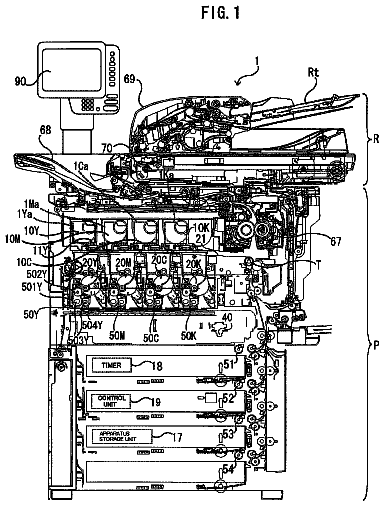
Timeline & family

Timeline From USPTO dates

20112013201520172019202120232025Application filedOct 12, 2010Application publishedMay 19, 2011Patent grantedNov 26, 20133.5-year fee paidMay 26, 20177.5-year fee paidMay 26, 202111.5-year fee not paidMay 26, 2025Patent expiredNov 26, 2025

Maintenance fees

Fees are due 3.5, 7.5 and 11.5 years after grant. This patent expired on November 26, 2025, so the fee marked "not paid" was the one that went unpaid.

3.5-year feeDue May 26, 2017Paid
7.5-year feeDue May 26, 2021Paid
11.5-year feeDue May 26, 2025Not paid

US family 2 documents, by filing date

Published applicationUS 2011/0116835 A1

SCANNING OPTICAL APPARATUS AND IMAGE FORMING APPARATUS USING THE SAME

Filed Oct 2010 · published May 2011
Published application
This documentUS 8,594,533 B2

Scanning optical apparatus and image forming apparatus using the same

Filed Oct 2010 · granted Nov 2013
Lapsed, fee not paid

Earlier publications, parents and continuations. None of them can still be enforced, or this patent would not be listed.

US patents it cites 5

Prior art cited by the examiner or applicant. Useful when you check your own idea for novelty.

Sources & verification

Verification

  • The USPTO Official Gazette of January 20, 2026 lists it as expired on November 26, 2025 for an unpaid maintenance fee.
  • It isn't on any reinstatement notice published since.
  • Its 1 US relative has also lapsed, expired or never issued.
  • Rechecked against USPTO records every day.
  • We check US rights only. Check foreign counterparts before selling abroad.

Confirm it yourself

  1. Open the file history on Patent Center.
  2. The status should read "Patent Expired Due to NonPayment of Maintenance Fees Under 37 CFR 1.362".
  3. Check the documents for any later petition to revive or reinstate.

Everything on this page comes from the documents linked above.

More in Cameras, Displays & Optics

All Cameras, Displays & Optics
Drawing from US 8,594,516 B2Lapsed, fee not paid9 drawings
Cameras, Displays & Optics · US 8,594,516 B2

Image forming apparatus and genuine product determining method for toner cartridge

An image forming apparatus includes: a loading unit on which a toner cartridge is loaded, the toner cartridge having a first storage unit in which first information indicating at least a date of manufacture of toner is…

Filed2010
LapsedNov 2025
OwnerKabushiki Kaisha Toshiba
Drawing from US 8,594,529 B2Lapsed, fee not paid10 drawings
Cameras, Displays & Optics · US 8,594,529 B2

Transfer unit engagement assembly of an image forming apparatus

An image forming apparatus includes a transfer unit detachably supported by a body frame to transfer an image on an image holding member to a recording medium.

Filed2010
LapsedNov 2025
OwnerSAMSUNG Electronics Co., Ltd.
Drawing from US 8,594,538 B2Lapsed, fee not paid13 drawings
Cameras, Displays & Optics · US 8,594,538 B2

Developing device and image forming apparatus

A developing device includes a developer tank and a developing roller.

Filed2012
LapsedNov 2025
OwnerSharp Kabushiki Kaisha
Drawing from US 8,594,539 B2Lapsed, fee not paid24 drawings
Cameras, Displays & Optics · US 8,594,539 B2

Outlet recess for a powder container for an image forming apparatus

An image forming apparatus includes: an inlet connected to an outlet of a container body for developer; a leakage preventing member arranged in the surroundings of the inlet and preventing leakage of the developer; and…

Filed2011
LapsedNov 2025
OwnerFuji Xerox Co., Ltd.