Background
1. Technical field
The invention relates to an electrophotographic photoreceptor, and an image forming apparatus and a process cartridge using the electrophotographic photoreceptor.
2. Related art
In recent years, in image forming apparatuses utilizing electrophotographic methods, halftone reproduction has been demanded due to the requirements of colorization and high definition. Accordingly, in an electrophotographic photoreceptor (hereinafter, may be abbreviated as "photoreceptor") used for image forming apparatuses, reproducibility of the halftone, namely, reproducibility of the exposure potential, is required.
Further, from the viewpoint of reduction in service costs, reduction in the frequency of replacement of the electrophotographic photoreceptor is required and, therefore, extension of the lifetime of the photoreceptors has become an important technical issue. Organic photoreceptors and inorganic photoreceptors are known as electrophotographic photoreceptors. Although organic photoreceptors are superior to inorganic photoreceptors in terms of cost or the like, organic photoreceptors are inferior to inorganic photoreceptors since the former have a short life due to abrasion of an organic photosensitive layer.
Thus, in order to lengthen the operating life of the organic photosensitive layer, provision of a protective layer with a high hardness and abrasion resistance on the surface of the organic photosensitive layer has hitherto been investigated.
Since a protective layer inhibits abrasion of the organic photosensitive layer, the lifetime of the organic photosensitive layer may be greatly extended. However, even if the protective layer has superior durability, it may be abraded with long-term use. For example, when a member such as a charging roll, a cleaning blade, or an intermediate transfer medium, which is directly in contact with the photoreceptor, is disposed at the periphery of the photoreceptor, or when hard particles such as silica or cerium oxide are used as an external additive for toner, the protective layer may be abraded.
Further, when a protective layer is provided at the surface of an organic photosensitive layer, and is irradiated with light emitted from a monochromatic light source such as a laser diode or light emitting diode, the irradiation causes reflection of light at the interface between the protective layer and the organic photosensitive layer. The occurrence of light reflection means that the amount of light is reduced when light incident on the surface of the photoreceptor reaches the photosensitive layer.
Summary
One aspect of the invention provides an electrophotographic photoreceptor including at least a photosensitive layer and a surface layer provided at the surface of the photosensitive layer, the surface layer including a first layer which is provided at a photosensitive layer side and has a refractive index of n1 and a second layer which is provided at an opposite side of the first layer to the photosensitive layer and has a refractive index of n2, and the photoreceptor satisfying the following Inequalities
to (3): |n0-n2|>0.1 Inequality
n0<n1<n2, or n0>n1>n2 Inequality
.lamda./(8.times.n1)+a.times..lamda./(2.times.n1).ltoreq.d1.ltoreq.3.time- s..lamda./(8.times.n1)+a.times..lamda./(2.times.n1) Inequality
wherein in Inequalities
to (3), n0 represents the refractive index of the photosensitive layer, n1 represents the refractive index of the first layer, n2 represents the refractive index of the second layer, d1 represents the film thickness (nm) of the first layer, a represents an integer of 0 or more, and .lamda. represents the wavelength (nm) of light with which the surface of the photoreceptor is irradiated when an electrostatic latent image is formed.
Brief description of the drawing
Exemplary embodiments of the invention will be described in detail based on the following figures, wherein:
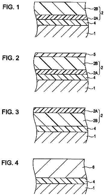
FIG. 1 is a schematic sectional view illustrating an example of the layer structure of a photoreceptor of an exemplary embodiment of the invention in which a surface layer having a two-layer structure is provided on the surface of the photosensitive layer;
FIG. 2 is a schematic sectional view illustrating an example of the layer structure of the photoreceptor of an exemplary embodiment of the invention;
FIG. 3 is a schematic sectional view illustrating another example of a layer structure of the photoreceptor of an exemplary embodiment of the invention;
FIGS. 4A and 4B are schematic views illustrating an example of a film-forming apparatus used when forming the surface layer of the photoreceptor of an exemplary embodiment of the invention;
FIG. 5 is a schematic view illustrating an another example of a plasma-generating unit that can be used in the film-forming apparatus shown in FIGS. 4A and 4B;
FIG. 6 is a plan view illustrating an image pattern of an original image on A4 size sheet of paper used in the evaluation in the Examples;
FIG. 7 is a schematic configuration diagram illustrating an example of an image forming apparatus of an exemplary embodiment of the invention; and
FIG. 8 is a schematic sectional view illustrating an example of the layer structure of a conventional photoreceptor, in which a single-layered surface layer is provided on the surface of the photoreceptor.
Detailed description
Electrophotographic Photoreceptor
The electrophotographic photoreceptor of the invention is an electrophotographic photoreceptor including a photosensitive layer and a surface layer provided at the surface of the photosensitive layer, the surface layer including a first layer which is provided at a photosensitive layer side and has a refractive index of n1 and a second layer which is provided at an opposite side of the first layer to the photosensitive layer and has a refractive index of n2, and the photoreceptor satisfying the following Inequalities
to (3): |n0-n2|>0.1 Inequality
n0<n1<n2, or n0>n1>n2 Inequality
.lamda./(8.times.n1)+a.times..lamda./(2.times.n1).ltoreq.d1.ltoreq.3.time- s..lamda./(8.times.n1)+a.times..lamda./(2.times.n1) Inequality
In Inequalities
to (3), n0 represents the refractive index of the photosensitive layer, n1 represents the refractive index of the first layer, n2 represents the refractive index of the second layer, d1 represents the layer thickness (mm) of the first layer, a represents an integer of 0 or more, and .lamda. represents the wavelength of light with which the surface of the photoreceptor is irradiated when an electrostatic latent image is formed.
Here, when the photosensitive layer is configured by plural layers (for example, when configured by a charge transport layer and a charge generation layer), the refractive index n0 refers to the refractive index of a layer provided at the surface layer side.
Further, the refractive indices n0, n1 and n2 are the refractive indices at the wavelength of light incident on a photoreceptor (in general, this refers to the wavelength of a monochromatic light source such as a laser or light emitting diode, but also indicates the maximum wavelength when a range of wavelengths are used), and in a medium with light absorption, the refractive index is represented by the real number part n in the equation of: double refractive index n*=n+ik.
In the measurement of the refractive index, the real number part n and the imaginary part k in the double refractive index are obtained by measuring .DELTA. and .phi. parameters which represent a state of polarized light measured by an ellipsometer, and which relate to the phase of the s and p polarized components and amplitude, respectively) at three incident angles in the range of from approximately 1,500 nm to approximately 200 nm with the use of a spectroscopic ellipsometer (trade name: M-2000, manufactured by J.A. Woollam Co. Inc.), and by analysis with analysis software WVAS32 and, further, the layer thicknesses d are determined. The samples used as specimens were obtained by forming only the layer to be measured on an Si substrate under conditions identical to the conditions when preparing the photoreceptor.
Further, the thickness of each layer is determined by observing cross-section images of the photoreceptor with a scanning electron microscope.
As described above, since the photoreceptor of the exemplary embodiment of the invention has a surface layer with a two-layer structure, and the refractive index and the layer thickness of each layer are set so as to satisfy Inequalities
to (3), generation of uneven surface potential at the surface of the photoreceptor after exposure may be suppressed, even when the surface of the photoreceptor is locally abraded. The principle according to which this effect may be attained will be explained with reference to the drawings.
FIG. 8 is a schematic sectional view illustrating an example of a layer structure of a conventional photoreceptor, in which a surface layer having a single layer structure is provided on the surface of the photosensitive layer and, more specifically, illustrating the interference of exposure light. In FIG. 8, 100 represents a photoreceptor, 110 represents a photosensitive layer, 120 represents a surface layer (single-layered surface layer), n0 represents the refractive index of the photosensitive layer 110, ns represents the refractive index of the surface layer 120, ds represents the thickness of the surface layer 120, R0s represents the reflected light component from the interface between the photosensitive layer 110 and the surface layer 120, Rsa represents the reflected light component from the surface of the surface layer 120, and n0.noteq.ns.
In the photoreceptor 100 of FIG. 8, although dependent on the layer thickness ds, the phases of the reflected light components R0s and Rsa are mutually weakened when both components are in an anti-phase condition, and the phases are mutually strengthened with when both reflected light components are completely in the in-phase condition. When local abrasion of the surface layer advances, the transmittance of the incident light varies depending on the location on the surface of the photoreceptor due to this kind of interference effect. Accordingly, when the difference between n0 and ns is large, uneven surface potential is consequently generated at the surface of the photoreceptor after exposure.
FIG. 1 is a schematic sectional view illustrating an example of a layer structure of a photoreceptor of the exemplary embodiment of the present invention, in which a surface layer having a two-layer structure is provided on the surface of a photosensitive layer and, more specifically, illustrating the interference of exposure light. In FIG. 1, 102 represents a photoreceptor, 110 represents a photosensitive layer, 121 represents a first layer, 122 represents a second layer, 123 represents a surface layer (a two-layered surface layer formed of the first layer 121 and a second layer 122), n0 represents the refractive index of the photosensitive layer 110, n1 represents the refractive index of the first layer 121, n2 represents the refractive index of the second layer 122, d1 represents the thickness of the first layer 121, d2 represents the thickness of the second layer 122, R01 represents a reflected light component from the interface between the photosensitive layer 110 and the first layer 121, R12 represents a reflected light component from the interface between the first layer 121 and the second layer 122, R2a represents a reflected light component from the surface of the second layer 122, and n0, n1 and n2 satisfy the relationship of n0>n1>n2, or, n0<n1<n2.
In the photoreceptor 102 of FIG. 1, while dependent on the layer thicknesses d1 and d2, interference occurs between the three reflected light components R01, R12 and R2a.
Here, when it is assumed that the reflected light components R01 and R12 are in the anti-phase condition,
if the reflected light components R01, and R12 are in the in-phase condition, R01 becomes anti-phase with respect to the reflected light components R2a and R12, and
if the reflected light components R2a and R01 are in the in-phase condition, R12 becomes anti-phase with respect to the reflected light components R2a and R01. Accordingly, even if local abrasion of the surface layer 123 advances, as long as the abrasion is generated within the second layer 122, any one of the components may act to suppress interference since the phases of the reflected light components do not all come into the in-phase condition, unlike the case shown in FIG. 8. Accordingly, even when the difference between n0 and n2 becomes large, the uneven surface potential generated at the surface of the photoreceptor after exposure may be suppressed. Furthermore, this effect may be obtained even when phases of the reflected light components R01 and R12 are not completely in the anti-phase condition, when the phases of the reflected light components R01 and R12 mutually canceling the interference to some extent.
In addition, a similar idea may be applied to a case in which the surface layer has a multilayer structure formed of three or more layers, or has an inclined structure such that the refractive index changes (increases or decreases) continuously toward the surface side of the surface layer from the photosensitive layer side in the thickness direction of the surface layer.
Hereinafter, the above Inequalities
to
will be explained in detail.
In the photoreceptor of the exemplary embodiment of the present invention, as shown in Inequality (1), the absolute value of the difference between the refractive index n0 of the photosensitive layer and the refractive index n2 of the second layer (hereinafter, also referred to as ".DELTA.n") is necessarily larger than 0.1. This is because the uneven surface potential after exposure which is generated at the surface of the photoreceptor due to the unevenness of the layer thickness of the surface layer cannot be generated unless a certain amount of difference in refractive index exists between the photosensitive layer and the surface layer.
When the second layer is formed from known materials for the surface layer, and the photosensitive layer is also formed from known materials for the photosensitive layer, most combinations of these materials may satisfy the difference in the refractive indices of Inequality (1). Representative examples include a case in which the photosensitive layer is formed from materials for an organic photosensitive layer or materials for an inorganic photosensitive layer, and the second layer is formed from inorganic materials for the above surface layer.
Accordingly, .DELTA.n is required to be larger than approximately 0.1, and is preferably approximately 0.2 or more.
Moreover, as shown in Inequality (2), the refractive indices of n0, n1 and n2 of the photosensitive layer, the first layer and the second layer, respectively, are required to satisfy a relationship such that the refractive indices increase or decrease in this order. When Inequality
is not satisfied, the effect may not be obtained since interference stronger than that produced in a single layer is caused
Furthermore, as shown in the following Inequality (4), in order to maximize the interference suppression effect among the three reflected light components, the value of the refractive index n1 is preferably around the mean value of the refractive index n0 and the refractive index n2. (n0+n2)/2-|(n0-n2)/4|.ltoreq.n1.ltoreq.(n0+n2)/2+|(n0-n2)/4| Inequality
In Inequality (4), n0 represents the refractive index of the photosensitive layer, n1 represents the refractive index of the first layer, and n2 represents the refractive index of the second layer.
When the diffractive index n1 is outside the above range, the interference suppression effect among the three reflected light components may not be obtained and, consequently, the uneven surface potential at the surface of the photoreceptor after exposure may occur. n1 is more preferably in a range of from (n0+n2)/2-|(n0-n2)/8| to (n0+n2)/2+|(n0-n2)/8|.
Further, in the exemplary embodiment of the present invention, the thickness d1 of the first layer is required to satisfy Inequality (3). In the first layer, the length corresponding to one cycle of the wavelength .lamda. of light (exposure wavelength) incident on the surface of the photoreceptor when forming an electrostatic latent image, is .lamda./(2.times.n1). Therefore, when the thickness d1 can assume a value close to an integral multiple of the above value (namely, when the thickness d1 is a value outside the range of Inequality (3)), the effect of canceling the interference among the reflected light components R01, R12 and R2a becomes insufficient, and uneven surface potentials after exposure may be generated at the surface of the photoreceptor.
Here, as shown in Inequality (3), the layer thickness d1 (nm) is required to be in a range of .lamda./(8.times.n1)+.lamda./(2.times.n1).ltoreq.d1.ltoreq.3.times..lamda- .(8.times.n1)+a.times..lamda./(2.times.n1), preferably in a range of 3.times..lamda./(16.times.n1)+a.times..lamda./(2.times.n1).ltoreq.d1.ltor- eq.5.times..lamda./(16.times.n1)+a.times..lamda./(2.times.n1), and is most preferably .lamda./(4.times.n1)+a.times..lamda./(2.times.n1).
In Inequality (3), a is not specifically limited, as long as a is an integer of 0 or more, and may be selected depending on the required thickness of the second layer. When the first layer is inferior in mechanical properties, light transmittance, electroconductivity or the like with respect to the second layer, a=0 is preferable in view of the properties.
The layer thickness of the second layer d2 is not specifically limited, but may be selected from the viewpoint of ensuring mechanical properties and abrasion tolerance, or suppressing absorption loss of light of the second layer. When the second layer is formed from an inorganic material, the thickness of the second layer is preferably from approximately 50 nm to approximately 2,000 nm, and more preferably from approximately 100 nm to approximately 1,000 nm. When the thickness d2 is less than approximately 50 nm, the abrasion tolerance is too small, and abrasion may proceed to the first layer if the photoreceptor is used over a long period of time. Since a location at which abrasion proceeds to the first layer is then in a similar condition to when a single-layered protective layer is formed on the photosensitive layer as shown in FIG. 8, an uneven surface potential after exposure may be generated at the surface of the photoreceptor. When the thickness d1 exceeds approximately 2,000 nm, the absorption loss of light caused by the second layer may become larger.
Further, when the second layer has a structure formed by dispersing filler in a resin or a resin matrix, from the viewpoint similar to the above, the thickness d1 is preferably from approximately 100 nm to approximately 20,000 nm, and more preferably from approximately 1,000 nm to approximately 10,000 nm.
Further, the invention may exert its effect when a difference in the layer thickness is caused in an evenly formed surface layer due to localized abrasion, and also exerts its effect when the difference in the layer thickness is caused at the time of layer formation.
Layer Structure of Photoreceptor
Hereinafter, the layer structure of the photoreceptor of the exemplary embodiment of the present invention is explained.
The photoreceptor of the exemplary embodiment of the present invention has a photosensitive layer and a surface layer provided on the photosensitive layer, and is not specifically limited as long as the surface layer includes a first layer and a second layer. The photosensitive layer is generally provided on a substrate having electroconductivity (electroresistivity being less than approximately 10.sup.13 .OMEGA.cm in volume resistivity; hereinafter, the same applies) (hereinafter, abbreviated as "conductive substrate"). If required, an intermediate layer such as a undercoat layer may be provided between the conductive substrate and the photosensitive layer.
The photosensitive layer may consist of two or more layers, or may be functionally separated. The photoreceptor of the exemplary embodiment of the present invention may be an amorphous silicon photoreceptor containing silicon atoms in the photosensitive layer, or an organic photoreceptor containing an organic polymer such as an organic photosensitive material in the photosensitive layer. Hereinafter, a specific example of the layer structure of a photoreceptor of an exemplary embodiment of the invention will be described in detail with reference to the drawings.
FIG. 2 is a schematic sectional view illustrating an example of the layer structure of a photoreceptor of an exemplary embodiment of the invention, wherein 1 represents a conductive substrate, 2 represents a photosensitive layer, 2A represents a charge generation layer, 2B represents a charge transport layer, and 3 represents a surface layer. In FIG. 2, a first layer and a second layer constituting the surface layer 3 are not shown (hereinafter, the same applies in FIG. 3).
The photoreceptor shown in FIG. 2 has a layer structure in which the charge generation layer 2A, the charge transport layer 2B, and the surface layer 3 are formed on the conductive substrate 1 in this order. The photosensitive layer 2 has a two-layered structure, formed of the charge generation layer 2A and the charge transport layer 2B.
FIG. 3 is a schematic sectional view illustrating another example of a layer structure of a photoreceptor of an exemplary embodiment of the invention, wherein 6 represents the photosensitive layer, 4 represents an undercoat layer, and the remainder is the same as shown in FIG. 2.
The photoreceptor shown in FIG. 3 has a layer structure in which the undercoat layer 4, the photosensitive layer 6 and the surface layer 3 are formed on the conductive substrate 1 in this order. The photosensitive layer 6 is a layer having integrated functions of both the charge generation layer 2A and the charge transport layer 2B shown in FIG. 2.
In the exemplary embodiment of the invention, the photosensitive layers 2 and 6 may be formed of an organic material or an inorganic material, or a combination thereof.
Organic Photoreceptor
Hereinafter, an exemplary embodiment of a preferable configuration of the photoreceptor of the invention in a case in which it is an organic photoreceptor will be described. The organic polymer compound included in the photosensitive layer may be thermoplastic or thermosetting, or may be formed by reacting two types of molecules.
In the case of an organic photoreceptor, the photosensitive layer may be a functionally separated layer having a charge generation layer and a charge transport layer as shown in FIG. 2, or a functionally integrated layer as shown in FIG. 3, In the case of a functionally separated layer, a charge generation layer may be formed at the surface side of the photoreceptor or a charge transport layer may be formed at the surface side.
Amorphous Silicon Photoreceptor
Hereinafter, an exemplary embodiment of a preferable configuration of the photoreceptor of the invention in a case in which it is an amorphous silicon photoreceptor will be described.
The amorphous silicon photoreceptor may be a photoreceptor for positive charging or negative charging. A photoreceptor, which is formed by coating an undercoat layer on a conductive substrate for blocking charge injection and improving adhesive property, and then coating a photoconductive layer and a surface layer thereon, may be used.
The top layer of the photosensitive layer (the layer on the surface layer side) may be p-type amorphous silicon or n-type amorphous silicon.
Surface Layer
Next, the surface layer is described in detail.
The surface layer provided on the surface of the photosensitive layer is not specifically limited, as long as the surface layer includes a first layer and a second layer.
In the photoreceptor according to an exemplary embodiment of the invention, the refractive indices and the layer thicknesses of the photosensitive layer, the first layer and the second layer are combined so as to satisfy the above Inequalities
to (3), so that interference between the reflected light components from the interfaces among these layers are suppressed, and generation of uneven surface potential at the surface of the photoreceptor after exposure is suppressed. To the extent that the action of this effect is not hindered, an intermediate layer may be provided, for example, at the lower side of the surface layer (namely, between the photosensitive layer and the surface layer), or between the first layer and the second layer. The refractive index of the intermediate layer is not specifically limited, but from the viewpoint that the action of the effect is not hindered, the thickness of the intermediate layer is preferably approximately 50 nm or less, and more preferably approximately 25 nm or less, depending on the refractive index of the intermediate layer.
As materials for forming the second layer at the surface side of the surface layer, the materials used for the surface layer of the photoreceptor may be used. As the materials, from the viewpoint of mechanical durability, for example, carbon materials such as amorphous carbon, oxide materials such as aluminum oxide and gallium oxide, or nitride materials such as carbon nitride may be used.
The amorphous carbon in an exemplary embodiment of the invention refers to an amorphous carbon hard film formed from mainly carbon and hydrogen atoms, and the concentration of hydrogen is approximately 60% or less. In general, the less the hydrogen content and the higher the sp3 carbon component ratio, the more the amorphous carbon is diamond-like and harder.
Of these materials, materials containing amorphous carbon, Ga, oxygen and hydrogen may be used. When these materials are used, in the photosensitive layer formed from an organic photosensitive layer, it becomes easy to satisfy Inequalities
and
and, as a result, generation of the uneven surface potential at the surface of the photoreceptor after exposure can be easily suppressed. Further, in consideration of suppression of an increase in residual potential on the photoreceptor during cyclic use, materials containing Ga, oxygen and hydrogen may be preferably used. The second layer formed from these inorganic materials may be either amorphous or crystalline.
For example, the refractive index of materials containing Ga, oxygen and hydrogen is from about 1.7 to about 2.0, and the refractive index of the amorphous carbon is from about 1.5 to about 2.4, although the refractive index of the above materials varies depending on the composition or production conditions thereof. The refractive index of the organic photosensitive layer is from about 1.5 to about 1.75, and the refractive index of the inorganic photosensitive layer (amorphous silicon layer) is from about 3.0 to about 4.0, although the refractive index varies depending on the composition thereof.
As the materials for forming the first layer at the photosensitive side of the surface layer, the materials used for the above-mentioned second layer may be used. When materials having a similar composition to those used in the second layer are used for the first layer, the composition of the materials configuring the first layer is selected so as to be slightly different from the composition of the materials configuring the second layer such that the refractive indices of the first and the second layers satisfy Inequality (2). When the compositions of materials for the first and second layers are the same, the film-forming conditions for the second layer is selected so as to be different from those for the first layer.
Of the first layer and the second layer of the surface layer, the second layer of the surface layer is generally required to have greater abrasion resistance and mechanical durability. For this reason, materials other than the above inorganic materials that have excellent abrasion resistance and mechanical durability may be used for the first layer as needed. Examples of such other materials include a resin material.
When the photosensitive layer is an organic photosensitive layer, examples of the combination of constituent materials of the first layer and the second layer include: (the first layer: the second layer)=(material containing Ga, oxygen and hydrogen:material containing Ga, oxygen and hydrogen); (amorphous carbon:amorphous carbon); (material containing Ga, oxygen and hydrogen:material containing Ga, nitrogen and hydrogen); and (material containing Al, oxygen and hydrogen:material containing Ga, oxygen and hydrogen).
Similarly, when the photosensitive layer is an inorganic photosensitive layer (amorphous silicon layer), examples of the combination of constituent materials of the first layer and the second layer include: (the first layer: the second layer)=(silicon carbide:silicon nitride).
Hereinafter, a case in which a material containing Ga, oxygen and hydrogen is used in the surface layer is explained in more detail.
The composition of the material containing Ga, oxygen and hydrogen is not specifically limited, but a composition of GaO.sub.x:H (x being in a range of about 1.1 to about 1.4) is particularly preferable from the following viewpoints:
the material may have an appropriate electroconductivity;
the material may suppress the increase in residual potential on the photoreceptor during cyclic use, even when the thickness of the surface layer exceeds about 0.2 .mu.m; and
the material may easily satisfy Inequalities
or
when the photosensitive layer is an organic photosensitive layer (in particular, an organic photosensitive layer containing a polycarbonate as a main component). In this case, from the viewpoint that Inequalities
or
are easily satisfied, the photosensitive layer (the layer at the surface side when the photosensitive layer has multilayer structure) is preferably an organic photosensitive layer containing a polycarbonate as a main component.
In the system that uses the composition of GaO.sub.x:H (x being in a range of about 1.1 to about 1.4), the electric resistance increases and the refractive index decreases with an increase in x. Accordingly, for example, when an organic photosensitive layer with a refractive index of approximately 1.65 is formed as the photosensitive layer and a surface layer is formed of the material having the composition of GaO.sub.x:H (x being in a range of about 1.1 to about 1.4), by setting x in the second layer at the surface side of the surface layer to be relatively small, and x in the first layer at the photosensitive layer side of the surface layer to be relatively large, the relationship of n2>n1>n0 may be satisfied.
Here, in this case, while an increase in the electric resistance in the first layer may adversely affect the electrical properties of the photoreceptor, this may be prevented by reducing the thickness d1 of the first layer to as thin as possible within the range of Inequality (3).
Further, in the system that uses the composition of GaO.sub.x:H (x being in a range of about 1.1 to about 1.4), as a method of controlling the refractive index, a method of adding carbon is exemplified, in addition to the method of controlling x. In this case, in order to reduce the refractive index, the addition amount of carbon is increased. For example, when an organic photosensitive layer with a refractive index of about 1.6 is formed as a photosensitive layer and the surface layer is formed of a material having the composition of GaO.sub.x:H (x being in a range of about 1.1 to about 1.4) with addition of carbon, by setting the amount of carbon in second layer at the surface side of the surface layer to be relatively low or to be carbon-free, and by setting the content of carbon in the first layer at the photosensitive layer side of the surface layer to be relatively high, the relationship of n2>n1>n0 may be satisfied.
Although an increase in the amount of carbon may cause deterioration in mechanical strength or abrasion resistance, shortening of the photoreceptor life does not occur since the deterioration in the above properties occurs within the first layer which does not constitute the surface of the surface layer.
In an exemplary embodiment of the invention, the contents of the elements such as Ga and oxygen in the surface layer and the distribution thereof in the film thickness direction are determined by Rutherford back scattering (hereinafter, referred to as "RBS" in some cases) in the following manner.
For RBS, an accelerator (trade name: 3SDH PELLETRON, manufactured by NEC corporation), an end station (trade name: RBS-400, manufactured by CE & A Co., Ltd.), and a system (trade name: 3S-R10) are used. The data is analyzed using HYPRA program (trade name, provided by CE & A Co., Ltd.).
As for RBS measuring condition, He++ ion beam energy is 2.275 eV; detection angle is 160.degree.; grazing angle with respect to incident beam is 109.degree..+-.2.degree..
The RBS measurement is specifically performed in the following manner.
First, He.sup.++ ion beam is irradiated vertically on a sample; a detector is placed at an angle of 160.degree. with respect to the ion beam; and the signal of He backscattered backward is determined. The composition ratio and the film thickness thereof are determined from He energy and intensity detected. The spectrum may be measured from two detection angles, for improvement in the measurement accuracy of composition ratio and film thickness. The measurement accuracy may be improved by crosschecking the results by measurement from two detection angles different in resolutions in the depth direction and backward scattering kinetics.
The number of He atoms scattered backward by the target atom depends only on three components: 1) the atomic number of target atom, 2) the energy of He atom before scattering, and 3) the scattering angle. The density is calculated from the measured composition, and the film thickness is calculated from the density. The error of density is not more than 20%.
The hydrogen content are determined by hydrogen forward scattering (hereinafter, referred to as "HFS" in some cases) in the following manner.
For HFS, an accelerator (trade name: 3SDH PELLETRON, manufactured by NEC), an end station (trade name: RBS-400, manufactured by CE & A Co., Ltd.), and a system (trade name: 3S-R10) are used. The data is analyzed using HYPRA program (trade name, provided by CE & A Co., Ltd.).
As for RBS measuring condition, He.sup.++ ion beam energy is 2.275 eV; detection angle is 160.degree.; grazing angle with respect to incident beam is 30.degree..
In HFS measurement, hydrogen signals scattered in front of a sample are collected by placing a detector at a position at an angle of 30.degree. with respect to the He.sup.++ ion beam, and placing a sample at an angle of 75.degree. with respect to the normal line. The detector is preferably covered with a thin aluminum foil to remove He atoms scattered with hydrogen. The amount is determined by comparing the hydrogen counts of a test sample with that of a reference sample after normalization with blocking power. The reference sample used is Si sample injected with H ion, or white mica. The white mica is known to have a hydrogen concentration of approximately 6.5 atomic %. The amount of H absorbed on the outmost layer can be calculated by subtracting the H amount adsorbed on a clean Si surface.
The elemental composition in the depth direction is determined by, for example, a method of collecting profile data of depth from the surface, a method of measuring the surface with the surface being etched by sputtering in a vacuum, or a method of mapping the composition of a sectional sample. The method may be selected in accordance with the analysis method.
Method of Forming the Surface Layer
Hereinafter, the method of forming the surface layer in the exemplary embodiment of the invention will be described. The surface layer may be formed by a known gas-phase film-forming method, such as a plasma CVD (chemical vapor deposition) method, an organometallic gas-phase growth method, a molecular beam epitaxy method, or a sputtering method. When the first layer provided at the photosensitive layer side of the surface layer is not formed of a hard inorganic material, in addition to the above film-forming methods, known liquid phase film-forming methods such as a dip coating method may be used.
When the surface layer has a two-layered structure as shown in FIG. 1, or has a multilayer structure formed of three or more layers, a different film-forming condition or a different film-forming method is applied for the formation of each layer so that the relationship in Inequality
may be satisfied.
When the surface layer has a structure with a continuously varying refractive index in the film thickness direction, the layer formation can be carried out such that the film-forming conditions are gradually changed with time during layer formation. Alternatively, after a surface layer with a single layer structure having a uniform composition in the film thickness direction is formed, a distribution in ion concentration in the film thickness direction of the surface layer is provided by injecting an ion to the surface of the surface layer, and the profile of the composition is controlled, thereby forming a surface layer with a continuously varying refractive index in the film thickness direction. Furthermore, the refractive index of amorphous carbon may be changed by irradiation with ions such as He and the like, or a radiation beam.
Hereinafter, an exemplary embodiment of an apparatus used in forming the surface layer will be described with reference to drawings.
FIGS. 4 A and 4B are schematic views illustrating an example of the film-forming apparatus used in forming the surface layer of the photoreceptor of an exemplary embodiment of the invention; FIG. 4A is a schematic sectional view illustrating the side view of the film-forming apparatus; and FIG. 4B is a schematic sectional view illustrating the film-forming apparatus shown in FIG. 4A as seen along the line A1 to A2. In FIGS. 4 A and 4B, 10 represents a film-forming chamber, 11 represents an exhaust vent, 12 represents a substrate-rotating unit, 13 represents a substrate holder, 14 represents a substrate, 15 represents a gas inlet, 16 represents a shower nozzle, 17 represents a plasma diffusion unit, 18 represents a high-frequency power supply unit, 19 represents a flat plate electrode, 20 represents a gas-supply tube, and 21 represents a high-frequency discharge tube unit.
In the film-forming apparatus shown in FIGS. 4 A and 4B, the exhaust vent 11 connected to a vacuum exhaust device not shown in Figures is connected to one terminal of the film-forming chamber 10, and a plasma-generating unit including a high-frequency power supply unit 18, the flat plate electrode 19 and the high-frequency discharge tube unit 21 is provided on the side opposite to the exhaust vent 11 of the film-forming chamber 10.
The plasma-generating unit has a high-frequency discharge tube unit 21, the flat plate electrode 19 placed in the high-frequency discharge tube unit 21 with its discharge face facing the exhaust vent 11, and the high-frequency power supply unit 18 placed outside the high-frequency discharge tube unit 21 and connected to the face opposite to the discharge face of the flat plate electrode 19. The gas-supply tube 20 for supplying a gas into the high-frequency discharge tube unit 21 is connected to the high-frequency discharge tube unit 21, and the other end of the gas-supply tube 20 is connected to a first gas supply source not shown in the Figures.
The description continues in the full USPTO document.
 Lapsed, fee not paid7 drawings