Patent Yard Sign in
Lapsed, fee not paid

Wafer level packaging

US 8,564,106 B2 · Assignee: Micron Technology, Inc. · Inventors: Chua; Swee Kwang et al.

USPTO PDF

Overview

Drawings on their way

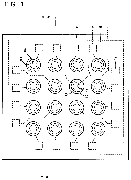
This patent has 14 drawing sheets. They are being downloaded; every one is in the USPTO PDF now.

Open the USPTO PDF

Full text on its way

This patent is listed from its USPTO record because it passed every check. Its abstract, claims and description are being downloaded from USPTO and will appear here within days. Until then, read it in the USPTO PDF or on Google Patents.

Why it's free to use

  • The USPTO Official Gazette of December 16, 2025 lists it as expired on October 22, 2025 for an unpaid maintenance fee.
  • It isn't on any reinstatement notice published since.
  • Its 7 US relatives have also lapsed, expired or never issued.
  • We check US rights only. Check foreign counterparts before selling abroad.
FiledJanuary 27, 2012
GrantedOctober 22, 2013
Expired (fee)October 22, 2025
Application number13/360044
Classification (CPC)H10W20/023 +7 more
Length26 pages

Drawings 14

The 14 drawing sheets are on the way. Every sheet is in the USPTO PDF.

Claims

On their way

The claims are being downloaded from USPTO and will appear here within days. Until then, read it in the USPTO PDF or on Google Patents.

Description

On its way

The description is being downloaded from USPTO and will appear here within days. Until then, read it in the USPTO PDF or on Google Patents.

Timeline & family

Timeline From USPTO dates

20032006200920122015201820212024Earliest priority dateAug 28, 2002Application filedJan 27, 2012Application publishedMay 17, 2012Patent grantedOct 22, 20133.5-year fee paidApril 22, 20177.5-year fee paidApril 22, 202111.5-year fee not paidApril 22, 2025Patent expiredOct 22, 2025

Maintenance fees

Fees are due 3.5, 7.5 and 11.5 years after grant. This patent expired on October 22, 2025, so the fee marked "not paid" was the one that went unpaid.

3.5-year feeDue April 22, 2017Paid
7.5-year feeDue April 22, 2021Paid
11.5-year feeDue April 22, 2025Not paid

US family 8 documents, by filing date

Published applicationUS 2003/0232488 A1

Wafer level packaging

Filed Aug 2002 · published Dec 2003
Published application
PatentUS 7,375,009 B2

Method of forming a conductive via through a wafer

Filed Aug 2002 · granted May 2008
Patent, expired (term ended)
Published applicationUS 2008/0211113 A1

WAFER LEVEL PACKAGING

Filed May 2008 · published Sep 2008
Published application
PatentUS 7,820,484 B2

Wafer level packaging

Filed May 2008 · granted Oct 2010
Patent, expired (term ended)
Published applicationUS 2011/0018143 A1

WAFER LEVEL PACKAGING

Filed Oct 2010 · published Jan 2011
Published application
PatentUS 8,106,488 B2

Wafer level packaging

Filed Oct 2010 · granted Jan 2012
Patent, expired (term ended)
Published applicationUS 2012/0119263 A1

WAFER LEVEL PACKAGING

Filed Jan 2012 · published May 2012
Published application
This documentUS 8,564,106 B2

Wafer level packaging

Filed Jan 2012 · granted Oct 2013
Lapsed, fee not paid

Earlier publications, parents and continuations. None of them can still be enforced, or this patent would not be listed.

US patents it cites 0

No US citations on record.

Sources & verification

Verification

  • The USPTO Official Gazette of December 16, 2025 lists it as expired on October 22, 2025 for an unpaid maintenance fee.
  • It isn't on any reinstatement notice published since.
  • Its 7 US relatives have also lapsed, expired or never issued.
  • Rechecked against USPTO records every day.
  • We check US rights only. Check foreign counterparts before selling abroad.

Confirm it yourself

  1. Open the file history on Patent Center.
  2. The status should read "Patent Expired Due to NonPayment of Maintenance Fees Under 37 CFR 1.362".
  3. Check the documents for any later petition to revive or reinstate.

Everything on this page comes from the documents linked above.

More in Chips & Semiconductors

All Chips & Semiconductors
Lapsed, fee not paidUS 8,564,103 B2
Chips & Semiconductors · US 8,564,103 B2

Method of manufacturing an electronic device

In order to protect IMD layers, particularly low-k dielectrics, a protection film is formed on the sidewall of an opening in the IMD layers prior to etching a trench in the underlying silicon substrate.
Filed2009
LapsedOct 2025
OwnerTaiwan Semiconductor Manufacturing Company, Ltd.
Lapsed, fee not paidUS 8,564,105 B2
Chips & Semiconductors · US 8,564,105 B2

Pin diode

A PIN diode having improved avalanche resistance is provided.

Filed2010
LapsedOct 2025
OwnerSansha Electric Manufacturing Co., Ltd.
Lapsed, fee not paidUS 8,564,178 B2
Chips & Semiconductors · US 8,564,178 B2

Micro electric generator, method of providing the same, and electric generating device

A micro electric generator is disclosed, which comprises: at least one electrically conductive fiber, and at least one piezoelectric ceramic layer covering on the surface of that at least one electrically conductive…

Filed2010
LapsedOct 2025
OwnerNational Tsing Hua University