Lapsed, fee not paid7 drawings
Hardware & Electronics · US 8,531,837 B2
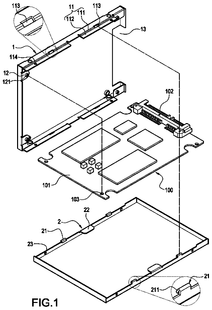
Pad mechanism capable of adjusting height thereof and electronic device therewith
A pad mechanism includes a step fixing structure having a plurality of step platforms.
US 8,531,862 B2 · Assignee: NXP B.V. · Inventors: Roest; Aarnoud Laurens et al.
Sheet 1 of 9 from the published document. All sheets in the USPTO PDF
The present invention relates to an electric component comprising at least one first MIM capacitor having a ferroelectric insulator with a dielectric constant of at least 100 between a first capacitor electrode of a first electrode material and a second capacitor electrode of a second electrode material. The first and second electrode materials are selected such that the first MIM capacitor exhibits, as a function of a DC voltage applicable between the first and second electrodes, an asymmetric capacitance hysteresis that lets the first MIM capacitor, in absence of the DC voltage, assume one of at least two possible distinct capacitance values, in dependence on a polarity of a switching voltage last applied to the capacitor, the switching voltage having an amount larger than a threshold-voltage amount. The invention is applicable for ESD sensors, memories and high-frequency devices.
U.S. Pat. No. 5,524,092 describes a multilayered ferroelectric-semiconductor memory device, in which two different values of the capacitance of the device are available, depending on the direction of the polarization of the ferroelectric layer. To this end, a ferroelectric-semiconductor interface is provided. Determining the capacitance of the structure allows to derive the polarization state of the ferroelectric layer without changing it. This way, information can be stored and nondestructively read. However, the layer structure of U.S. Pat. No. 5,524,092 is rather complicated. Furthermore, it has been proven technologically difficult to fabricate layer structures with a semiconductor material such as silicon adjacent to a ferroelectric. This reduces the choice of materials and requires the use of materials, which are not typically integrated into an industrial fabrication process. This
1 of 9 drawing sheets so far from the published document, cropped to the drawing. Every sheet is in the USPTO PDF.
What the patent claimed, word for word. All of it is now free to use.
The present invention relates to an electric component comprising a ferroelectric MIM capacitor. A ferroelectric MIM capacitor is a capacitor of the metal-insulator-metal type with a ferroelectric insulator. The invention also relates to a method for detecting electrostatic discharge (ESD) events and to a corresponding a ESD sensor device comprising the subject electric component. Furthermore, the invention relates to a ferroelectric memory, which comprises the subject electric component, and to a method for reading from the ferroelectric memory. The subject matter disclosed in the document US 2002/0177326 A1 is incorporated herein in its entirety.
U.S. Pat. No. 5,524,092 describes a multilayered ferroelectric-semiconductor memory device, in which two different values of the capacitance of the device are available, depending on the direction of the polarization of the ferroelectric layer. To this end, a ferroelectric-semiconductor interface is provided. Determining the capacitance of the structure allows to derive the polarization state of the ferroelectric layer without changing it. This way, information can be stored and nondestructively read. However, the layer structure of U.S. Pat. No. 5,524,092 is rather complicated. Furthermore, it has been proven technologically difficult to fabricate layer structures with a semiconductor material such as silicon adjacent to a ferroelectric. This reduces the choice of materials and requires the use of materials, which are not typically integrated into an industrial fabrication process. This in turn increases the processing cost.
U.S. Pat. No. 5,262,983 discloses a memory comprising a ferroelectric capacitor. Application of an external voltage generates respective space charge regions proximate to a respective interface between the ferroelectric and each electrode. Sandwiched between the space charge regions, an uncharged region of the ferroelectric remains. The ratio of the extensions of the uncharged regions of the ferroelectric material and of the space charge regions in the direction of the layer sequence influences the capacitance. A hysteresis of the capacitance vs. voltage is effected by a superposition of the internal polarization of the ferroelectric and of the polarization of the space charge regions under application of an external electric field. A number of distinguishable, stable states for storing values can be provided this way.
A write signal has a bias voltage greater than the coercive voltage of the ferroelectric layer. Two situations can be distinguished: a) The bias voltage establishes an electric field that is additive with the internal polarization field. This increases the size of the space charge region, with a concomitant decrease in capacitance. b) The bias voltage establishes an electric field that is subtractive to the internal polarization field. This decreases the size of the space charge region, with a concomitant increase in capacitance.
The actual capacitance value assumed by the capacitor depends on the history of the bias voltage. A larger capacitance is achieved after scanning the bias voltage to a negative voltage larger than the coercive field. A smaller capacitance is achieved by scanning the bias voltage to a positive value larger than the coercive field of opposite polarity.
There are several issues that render the device described in U.S. Pat. No. 5,262,983 undesirable for application in the field.
First, if the space charges are immobile at high frequency, then the full layer stack will always have the same capacitance. Accordingly, the space charge regions have to be electrically conductive at the desired frequency of operation. They in effect behave as semiconductor regions. It is known that ferroelectric materials can be made semiconductive. Semiconductor materials allow the formation of a depletion layer, which can act as a capacitance sensor. In other words, in the device of U.S. Pat. No. 5,262,983, the capacitance is not defined by the neutral zone in the ferroelectric layer, but by the extension of the depletion layer in the space-charge region. As a result, the layer structure of this document resembles that of U.S. Pat. No. 5,524,092 and shares its disadvantage of high complexity.
Second, in the device of U.S. Pat. No. 5,262,983, a non-zero bias voltage has to be applied in a read operation to differentiate between capacitance states.
It would be desirable to provide a capacitive structure for an electric component that does not require the application of a bias voltage for determining the capacitance state.
According to a first aspect of the invention, an electric component is provided that comprises: at least one first MIM capacitor having a layer structure including a ferroelectric insulator with a dielectric constant of at least 100 between a first capacitor electrode of a first electrode material and a second capacitor electrode of a second electrode material; wherein the first and second electrode materials are selected such that the first MIM capacitor exhibits, as a function of a DC voltage applicable between the first and second electrodes, an asymmetric capacitance hysteresis that lets the first MIM capacitor, in absence of the DC voltage, assume one of at least two possible distinct capacitance values, in dependence on a polarity of a switching voltage last applied to the capacitor, the switching voltage having an amount larger than a threshold-voltage amount; and a circuit, which is operably connectable to the MIM capacitor and which is configured to generate and provide an output signal, which depends on the capacitance value of the at least one first MIM capacitor assumed in absence of the DC voltage on the first MIM capacitor or at an amount of the DC voltage on the first MIM capacitor, which is smaller than a quarter of a voltage difference between a positive and a negative coercive voltage associated with the ferroelectric insulator layer of the first MIM capacitor.
The electric component of the invention achieves a particularly strong hysteresis asymmetry of the capacitance of the first MIM capacitor as a function of an applied DC bias voltage, meaning that the maximum of the capacitance-voltage curve occurs at different DC bias voltages depending on the bias history. This gives rise to a particularly strong capacitance contrast at and near a DC bias voltage of 0 V for the different bias histories. This in turn leads to the possibility of reading out a bias history of the ferroelectric MIM capacitor even without having to apply a bias voltage. A wide range of applications for the electric component is opened up, which will be described by way of embodiments hereinafter.
The electric component of the present invention has the further advantage that a particularly long lifetime of the MIM capacitor and thus of the electric component is achieved by generating and providing an output signal, which depends on the capacitance value of the at least one first MIM capacitor either assumed in absence of the DC voltage on the first MIM capacitor or at the very small DC voltage (i.e., in the above-mentioned meaning).
A DC voltage in the present context of a capacitance measurement is considered a voltage, which is constant throughout the capacitance measurement or, if changing in time at all, which has a rate of relative voltage change over the duration of the capacitance measurement, which is smaller than the reciprocal value of the duration of the capacitance measurement. The term "relative" refers to the maximum bias voltage applicable to the MIM capacitor as a reference.
The coercive voltage is a respective positive or negative voltage value, which is a characteristic of a given ferroelectric insulator layer in the first MIM capacitor. It is a technical parameter well known in the art.
The wording "in absence of a DC voltage" refers to a DC bias voltage of 0 V. A DC bias voltage smaller than a quarter of a voltage difference between a positive and a negative coercive voltage associated with ferroelectric insulator layer of the MIM capacitor will herein also be referred to as a "very small DC voltage" or a "very small DC bias voltage" or a "very small bias voltage".
Furthermore, the electric component is suitable for applications even without external power supply.
In the following, embodiments of the electric component will be described by way of their features, which are provided in addition to those of the electric component of the present invention. Additional embodiments can be derived by combining the additional features of different embodiments with each other, unless such a combination is excluded explicitly or implicitly, namely by facts known to the person of ordinary skill in the art, that the additional features can only be realized as alternatives to each other.
The term "ferroelectric insulator" is to be understood as comprising in different embodiments a ferroelectric or an anti-ferroelectric material. In the art, the term ferroic is sometimes used as a generic term that encompasses both alternatives for spontaneous polarization, including a coupling to magnetic polarization.
The at least two capacitance values of the at least one first MIM capacitor that can be assumed in the absence of the DC voltage between the capacitor electrodes are distinct in the sense that they differ from each other by an amount that allows distinguishing between the assumed capacitance values in the output signal of the circuit, which output signal depends on the capacitance value assumed in absence of the DC voltage. In one embodiment, the capacitance values, in absence of the applied DC voltage, i.e., at zero voltage, differ by at least 5% from each other. That means, the lowest of the two or more possible capacitance values is at most 95% of the highest value. In another embodiment, they differ by at least 10% from each other. In a further embodiment, the difference between the lowest and he highest capacitance value is about 20% of the highest capacitance value.
The threshold-voltage amount required for changing the capacitance value, which is assumed in absence of the DC voltage, correlates with the coercive field that must applied to the ferroelectric insulator of the first MIM capacitor in a particular capacitor structure. Typical values for the threshold-voltage amount range between 1 and 20 V. However, this is not to be understood as a restriction. The first MIM capacitor may be designed to exhibit another desired threshold-voltage amount.
Typically, as is well known from the physics of ferroelectric materials, the switching voltage must also have a specific polarity, depending on the capacitance value currently assumed by the first MIM capacitor. If an unsuitable switching-voltage polarity is used, the capacitance value, as measured in the absence of the DC voltage or at the very small DC voltage, will not change.
One way to achieve a hysteresis with the characteristics of the MIM capacitor of the electric component of the present invention is to provide a first and a second capacitor electrode, the first and second electrode materials of which are metals and differ from each other at least by having different work functions. As is well known, the work function of a metal is the energy needed to move an electron from the Fermi energy level of the metal into a vacuum. This parameter that characterizes a given metal, is well known in the art for many metals.
In one particular form of this embodiment, the first capacitor electrode is made of Ti/Pt and the second capacitor electrode is made of TiW. TiW has a lower work function than Ti/Pt, and it is preferably used as a material for a top electrode as opposed to a bottom electrode disposed on a substrate.
However, this embodiment forms only a non-restrictive example. Other metals can be used. It should be noted that it is possible to even use the same metal and apply different fabrication conditions or different treatment to the electrodes in order to achieve different work functions in the respective electrode materials. This simplifies the fabrication of the first MIM capacitor in the context of the fabrication of the electric component.
For some applications, consideration should be given to the fact that many ferroelectric materials gradually change their hysteresis characteristics during the lifetime of the electric component. To avoid false interpretation of the output signal of the circuit, one embodiment of the electric component further comprises: a second MIM capacitor having a capacitance-voltage hysteresis of the same kind as the first MIM capacitor. In the electric component, the first electrode of the first MIM capacitor and the second electrode of the second MIM capacitor are both connected to a reference potential; the switching voltage is applicable in parallel to the second electrode of the first MIM capacitor and to the first electrode of the second MIM capacitor; and the capacitance-sensor unit is configured to generate first and second capacitance sensor signals indicative of the capacitance values in the absence of the DC voltage, of the first and of the second MIM capacitors, respectively.
The referenced potential is in one embodiment a ground potential or mass.
The provision of two MIM capacitors with the described opposite connections allows applying the switching voltage between the second electrode of the first MIM capacitor and the first electrode of the second MIM capacitor. Since the capacitance of the MIM capacitor will only change if the applied switching voltage has a negative polarity, the two capacitors are put in an anti-parallel configuration. In this configuration, one of the two capacitors will always experience the applied switching voltage as negative and therefore change its capacitance value. In this way, it is possible to simultaneously register the sign and the energy of an applied switching signal. It is also possible to reset both capacitors after the application of a switching voltage in order to be able to register a next switching event.
Suitably, the circuit of the electric component forms a part of, or, in the alternative, fully forms a capacitance-sensor unit, which is configured to generate and provide at its output a capacitance-sensor signal. The capacitance-sensor signal is indicative of the momentaneous or current capacitance value in the absence of DC voltage of the at least one first MIM capacitor. With a capacitance-sensor unit, the electric component is suited for a wealth of applications that employ a switching of the capacitance value in the absence of the DC voltage in sensor device.
More specifically, as an example of a circuit that only is a part of a capacitance-sensor unit, the circuit may be configured to measure and provide at its output a momentaneous value of an electrical quantity of the first circuit that depends on the capacitance of the MIM capacitor. The capacitance-sensor unit in turn may be configured to derive from the measured momentaneous value of the electrical quantity a capacitance-sensor signal indicative of the momentaneous capacitance value of the MIM capacitor. This capacitance-sensor signal is provided as an output of the capacitance-sensor unit.
The electric component of this embodiment is useful in many applications, including memory applications and ESD sensor applications. This will be elucidated in the course of the description of further embodiments.
For some applications, a single first capacitor is enough. However, since a capacitance switching is achieved with a switching voltage of a predetermined switching-voltage polarity, a detection of an occurrence of a desired or of an undesired and unexpectedly high voltage of the polarity opposite to the switching-voltage polarity would not be possible if only a single first MIM capacitor is used.
If occurrence of a high voltage (i.e., larger than the switching voltage,) is to be detected with sensitivity also to the voltage polarity, a further embodiment of the electric component, which comprises a second MIM capacitor, is useful. The first and second MIM capacitors are connected to each other in an antiparallel configuration. By detecting the capacitances of the first and second MIM capacitors in their anti-parallel configuration, both voltage polarities can be detected. For a capacitance change is only observed if a switching voltage polarity (typically a negative voltage polarity) is applied. By providing two MIM capacitors in an antiparallel configuration, one of the two will always experience an applied voltage as negative, thus allowing to simultaneously register sign and energy of the (ESD) voltage.
In this anti-parallel configuration, the first electrode of the first MIM capacitor and the second electrode of the second MIM capacitor are suitably connected to ground. The switching (or ESD) voltage is applicable between the second electrode of the first MIM capacitor and the first electrode of the second MIM capacitor. The second MIM capacitor is suitably of the same type as the first MIM capacitor.
The capacitance-sensor unit of this type of embodiment of the electric component is configured to individually measure the capacitance of the first and second MIM capacitors and to derive first and second capacitance sensor signals indicative of the capacitance of the first and of the second MIM capacitor, respectively.
Preferably, the capacitance-sensor unit is additionally configured to derive and provide a polarity-sensor signal indicative of the polarity of the switching voltage, from the measured capacitances. The polarity information can for instance be determined from a comparison of the capacitance values of the first and second MIM capacitors. Thus, the capacitance-sensor unit is suitably configured to compare the capacitance values for the first and second MIM capacitors and to provide a polarity information indicative of the a polarity of the switching voltage last applied to the MIM capacitor, in dependence on the result of the comparison. Of course, the provided polarity information can be integrated into one of the capacitance sensor signals.
The measured capacitances of the first and, if of the same type according to the present invention, also the second MIM capacitor are indicative of the bias histories of the capacitors in the sense that an energy of a bias voltage last applied can be detected. For ESD sensor applications, a detection of an energy amount delivered by an ESD pulse may be useful to assess a probability of damage to an electronic circuit. To this end, one embodiment comprises an ESD evaluation unit. The ESD evaluation unit is connected with the capacitance-sensor unit of the electric component and configured to derive from the capacitance-sensor signals information on an energy amount and polarity provided to the ESD sensor by the electrostatic discharge event.
It is possible to reset the ESD sensor after an ESD event to be able to register the next ESD event based on the same voltage-dependent capacitance behavior. To this end, an embodiment of the ESD sensor comprises a reset unit, which is connected with the capacitance sensor unit. The reset unit is configured to provide, after a detection of the capacitance of the first MIM capacitor or the second MIM capacitor having assumed the respective lower capacitance value, a reset voltage of a reset-voltage amount and a reset voltage polarity to the first and/or second capacitor, respectively, such that the first and second MIM capacitors both re-assume their respective higher capacitance value.
In other applications, it may be desired to provide an electric component, which is able to provide different capacitance values, and to allow a switching between these capacitance values. Accordingly, one embodiment of the electric component comprises: a switching unit, which is either connected or connectable with the at least one first MIM capacitor and which is configured to provide one of two alternative switching voltages of suitable polarity and of a suitable amount for switching the capacitance of the at least one first MIM capacitor between a lower and a higher capacitance value, depending on the momentaneous capacitance value assumed by the first MIM capacitor. This way, a reversible switching between the lower and the higher capacitance values is achievable. The switching-voltage amount should be selected to exceed the coercive field.
This embodiment, if combined with the previously described embodiment, which additionally comprises a capacitance-sensor unit, allows building a ferroelectric memory. An advantage of this ferroelectric memory structure is that it allows a non-destructive readout. Furthermore, the memory is non-volatile.
A ferroelectric memory based on the present invention further comprises in one embodiment a plurality of first MIM capacitors, each associated with an address and each being configured to store at least one respective bit of information in the form of a respective capacitance value assumed in absence of a DC voltage applied between the capacitor electrodes, a read unit, which comprises the capacitance-sensor unit and has an input for receiving address information indicative of at least one of the first MIM capacitors to be read; and a write unit, which comprises the switching unit, and which has an input for receiving write information to be written to the memory, and address information indicative of at least one of the first MIM capacitors to be written to.
The read unit will in operation generate and provide at its output a capacitance-sensor signal for each of the MIM capacitors indicated by the address information. The output of the read unit is an information signal having information bits corresponding to the respective momentaneous capacitance values assumed in absence of a DC voltage. The write unit, in operation, provides a switching signal if a state of a memory cell is to be changed according to received write information and received address information. Further embodiments of a ferroelectric memory will be presented further below in the context of the description of the enclosed drawings.
A further application case of the electric component of the first aspect of the invention is a radio-frequency (RF) component. Two preferred application case of the RF component are described in the following: a) In a first preferred application case of the RF component, the circuit of the electric component of the first aspect of the present invention is configured to generate an output signal with a frequency that depends on the capacitance of the MIM capacitor in the absence of the DC voltage.
The RF component of this type allows tuning the frequency. This ability is advantages in many application contexts. Exemplary RF components of this type form or comprise oscillators, like for instance voltage-controlled oscillators (VCOs). Mobile telephones for instance have to provide capability for operation at more and more different frequencies. Using the RF component of the present embodiment, a reconfigurability is achieved, which allows omitting dedicated receiving and transmitting circuitry for all different frequencies of operation. Instead, a single receiving and transmitting circuitry can be used and tuned to a desired frequency. b) In a second application case of the RF component, additionally or alternatively to the first application case, a response of the RF component to RF signals depends on the capacitance of the MIM capacitor in the absence of the DC voltage on the first MIM capacitor or at an amount of the DC voltage on the first MIM capacitor, which is smaller than a quarter of a voltage difference between a positive and a negative coercive voltage associated with the ferroelectric insulator layer of the first MIM capacitor. The response of the RF component can also be described as an output signal detectable at an output of the RF component. Exemplary RF components of this type form comprise filters or matching networks.
As has become clear from the previous description, the electric component of the present invention can be used in many application contexts. Correspondingly, different electronic components form embodiments of the present invention. The invention can thus be used to provide a technology platform for a large number of different electronic components containing integrated asymmetric ferroelectric MIM capacitors.
An electronic components according to a preferred embodiment advantageously comprises a semiconductor substrate with an integrated circuit having at least one electric component according to the first aspect of the invention or one of its embodiments disclosed, and one or more of the following components integrated in or on the substrate: a resistor; a ferroelectric capacitor; an ESD protection diode; or an active integrated circuit.
The ferroelectric capacitor of the electronic component has in one embodiment a different structure than the first MIM capacitor of the electric component of the first aspect of the invention. In particular, such embodiments have ferroelectric MIM capacitors with a symmetric instead of an asymmetric capacitance hysteresis, implying particularly that at zero bias voltage there is only one capacitance value assumed irrespective of the voltage history the capacitor has experienced.
A preferred embodiment of the electronic component has the previously described ESD-sensor embodiment of the electric component (also defined in claim 6) integrated on the substrate. A further embodiment has an integrated memory forming the active integrated circuit. The memory can for instance take the form of the above-described ferroelectric-memory embodiment of the electric component (also defined in claim 11). The resistor can be formed as an integrated thin film resistor containing an alloy of one or more elements of Mo, Ni, Cr, Ti, Si or W or from a semiconducting material such as Si. Such resistors can be arranged on top of integrated ferroelectric MIM capacitors on the same substrate to save chip area. In particular, such thin-film resistors can at the same time form an electrical interface to the ferroelectric capacitor.
A further embodiment has the electric component in the form of an RF component as described in the previous description (also defined in claim 12) integrated on the substrate. It is understood that the electronic component may comprise a plurality of each of the components mentioned, or a combination of at least two different embodiments of the electric component of the first aspect of the invention.
The electronic component of the present invention provides an integration of the electric component with the integrated circuit on a single substrate. Of course, a combination of such a substrate with other substrates, for instance in a System-in-package, is possible, to form more complex IC packages.
A further aspect of the present invention is formed by a method for detecting an occurrence of an ESD event in an electronic component. The method comprises: providing the electronic component with an ESD sensor according one of the ESD-sensor embodiments described herein; and ascertaining the capacitance of the at least one first MIM capacitor, in the absence of a DC voltage applied to the electrodes of the at least one first MIM capacitor.
A further aspect of the invention is formed by a method for reading from a ferroelectric memory. The method comprises: providing a ferroelectric memory according one of the ferroelectric-memory embodiments described herein; receiving address information of at least one memory cell to be read from; ascertaining the capacitance of the at least one first MIM capacitor of the at least one memory cell indicated by the address information, in the absence of a DC voltage applied to the electrodes of the at least one first MIM capacitor.
Preferred embodiments of the invention are defined in the dependent claims.
The present invention is further elucidated by the following Figures and examples, which are not intended to limit the scope of the invention. The person skilled in the art will understand that various embodiments may be combined.
These and other aspects of the invention will be apparent from and elucidated with reference to the embodiment(s) described hereinafter. In the following drawings:
FIG. 1 is a schematic cross-sectional view of a section of an electronic component with a semiconductor substrate and an integrated circuit that comprises an electric component with at least one MIM capacitor.
FIG. 2 shows a simplified circuit diagram of a second embodiment of an electric component.
FIG. 3 is a diagram, which plots the ratio between a measured capacitance of a MIM capacitor with a prior-art design having symmetric electrode properties and a reference capacitance value as a function of a bias DC voltage applied between the capacitor electrodes.
FIGS. 4 and 5 show capacitance-voltage hysteresis curves for a MIM capacitor of an electric component in accordance with the present invention.
FIG. 6 shows a simplified circuit diagram of an electric component according to a further embodiment of the present invention, which can be used as an ESD sensor.
FIGS. 7 to 10 are simplified circuit diagrams of different embodiments of electric components implementing at least two ferroelectric MIM capacitors.
FIG. 11 is a simplified circuit diagram for illustrating an embodiment of an electric component of the present invention, which can be used as a capacitance detection circuit, a ferroelectric memory, or an ESD sensor.
FIG. 12 is a simplified circuit diagram of an example of a read-out circuit for use with a ferroelectric MIM capacitor in a ferroelectric memory.
FIG. 13 is a further alternative embodiment illustrating a circuit section for reading out a ferroelectric memory using a ferroelectric MIM capacitor according to the present invention.
FIG. 14 provides a further alternative embodiment of a read out circuitry for a ferroelectric memory using two ferroelectric MIM capacitors according to the present invention.
FIGS. 15 and 16 are schematic and simplified circuit diagrams of ferroelectric memory devices according to further embodiments of an electric component of the present invention.
FIG. 1 is a schematic cross-sectional view of a section of an electronic component with a semiconductor substrate and an integrated circuit that comprises an electric component with at least one MIM capacitor. The electronic component 100 has a semiconductor substrate 102. The semiconductor substrate 102 may for instance be a silicon substrate. However, other substrate materials, such as III-V semiconductor substrates or other group-IV substrates such as SiGe or SiC substrates may be used, depending on the desired application. The substrate may also be a layered structure, such as in a silicon-on-insulator substrate. Only the uppermost substrate section of the substrate 102 is shown in FIG. 1.
The embodiment of FIG. 1 comprises a capacitor 104, a resistor 106 and a diode 108. An insulating layer 110 is deposited on the substrate 102. The insulating layer may for instance be formed of SiO.sub.2 or SiN. A barrier layer 112 is deposited on the insulating layer 110. The barrier layer 112 may for instance be made of SiN, SiO.sub.2, TiO.sub.2, Al.sub.2O.sub.3, HfO.sub.2, MgO, ZrO.sub.2, or a combination of these materials. On the barrier layer, a first capacitor electrode 114 of a first electrode material is formed. The first capacitor electrode is laterally structured and thus limited in its lateral extensions according to the needs of the specific capacitor design. The material of the first capacitor electrode 114 is metallic. In one embodiment, the first electrode comprises a Ti/Pt layer structure. For instance, a Ti layer with a thickness of 1-50 nm may by followed by Pt layer with a thickness of 20-600 nm. Alternatively, the first capacitor electrode 114 may be made of Pt only or Ti only. Furthermore, admixtures of W, Ru, Ir, N, Al, Ag, Rh, Cr, Si, alone or in combination, are suitable materials for the first capacitor electrode 114. The overall thickness of the first electrode may be chosen between 50 nm and 1 .mu.m.
On top of the first capacitor electrode layer 114, a dielectric layer 116 is deposited. The dielectric layer 116 is made of a ferroelectric material having a dielectric constant of at least 100. The dielectric constant of a material is also known in the art as the relative permittivity. For the purpose of the present specification it is the relative-permittivity value at a given measurement frequency in the range between 0.1 kHz and 1000 kHz.
The material of the dielectric layer 116 may for instance be PbZr.sub.xTi.sub.i-xO.sub.3 (0.ltoreq.x.ltoreq.1) with or without dopants such as La and/or Mn and/or Nb, and with or without excess Pb. The dielectric layer 116 may also be formed of a layered structure of different materials, differing for instance in the fraction of the different atoms in the above mentioned PZT or PLZT materials. Other ferroelectric materials are well known in the art and can be used for the dielectric layer 116 as well. Reference is for instance made to paragraphs
to
of US 2002/0177326 A1, wherein on page 3, left column, suitable dielectric materials for a "first dielectric layer 7" are mentioned. The ferroelectric materials mentioned there can also be used for the dielectric layer 116 of the present embodiment.
On top of the ferroelectric layer 116, a resistance layer 118 is provided, which together with a current supply lead 120 provides an electrical contact path to the bottom electrode 114. The resistance layer 14 may comprise, for example, .beta.-Ta, tantalum nitride, polysilicon, Ni.sub.xCr.sub.y (0.ltoreq.x, y.ltoreq.1), Ti.sub.xW.sub.y (0.ltoreq.x, y.ltoreq.1), or other suitable resistance material known in the art.
In a lateral neighborhood of the current supply lead 118/120, a second or top electrode 122 is arranged on the dielectric layer 116. The top electrode layer 122 is suitably made of TiW. The material choice of the first and second electrode materials is such that the MIM capacitor 104 exhibits, as a function of a DC voltage applicable between the electrodes, an asymmetric capacitance hysteresis that lets the MIM capacitor, in absence of the DC voltage, assume one of at least two possible distinct capacitance values, in dependence on a polarity of a switching voltage last applied to the capacitor, the switching voltage having an amount larger than a threshold-voltage amount. The asymmetric capacitance hysteresis of the MIM capacitor 104 is described in more detail with reference to FIGS. 4 and 5. A suitable choice of the second or top electrode material is TiW, whereas a suitable choice of the bottom electrode is Ti/Pt. However, it should be noted that other material combinations are suitable as well. In particular, it is not an essential feature to use different materials. The inventors have observed that the capacitance hysteresis according to the present invention can also be achieved by processing normally identical materials in a different way during the fabrication process. For instance, the layers of the first electrode 114 and of the second electrode 122 may be deposited at different temperatures. At present, it seems that it is enough to achieve a difference in the work functions of the electrode materials of the first and second electrode to provide the desired asymmetric capacitance hysteresis according to the present invention.
The top electrode is covered by a protective layer 124, such as polyimide, SiO.sub.2, SiN(H), or polybenzocyclobutene.
In the diode section 108 of the electric component 100, a diode is formed by adjacent p and n conductive layers 126, and 128, respectively. The diode is arranged in the silicon substrate 102 and contacted in very much the same way as the bottom electrode 114 of the ferroelectric MIM capacitor 104, namely, by a current lead 130, in combination with a resistive layer 132.
FIG. 2 shows a simplified circuit diagram of a second embodiment of an electric component 200. The electronic component 200 has two MIM capacitors 202 and 204, for instance of the type shown on FIG. 1, which are in anti-parallel connection with each other. That is, both MIM capacitors 202 and 204 have a capacitance-voltage hysteresis of the same kind as described for the MIM capacitor 104 of FIG. 1. The anti-parallel connection of the capacitors is realized by connecting a bottom electrode 202.1 of the MIM capacitor 202 to a top electrode 204.2 of the second MIM capacitor 204. These two electrodes 202.1 and 204.2 are connected in parallel to a input terminal 206. Both remaining electrodes, i.e. a top electrode 202.2 of MIM capacitor 202 and bottom electrode 204.1 of MIM capacitor 204 are connected to a reference potential, which for instance is ground potential. A capacitance-sensor unit, which is not shown in FIG. 2 is configured to generate corresponding capacitance-sensor signals, which indicate the capacitance values in absence of a DC voltage of each of the MIM capacitors 202 and 204, respectively. Because a capacitance change will only be observed, if an applied bias voltage applied via the input terminal 206 has a given polarity, typically a negative polarity, the anti-parallel configuration of the two-MIM capacitors 202 and 204 ensures that always one of the two capacitors will experience the applied voltage as negative and therefore change its capacitance value. In this way, it is possible to simultaneously register the sign and the energy of an input voltage received via the signal input terminal 206, which could for instance an ESD pulse, or an otherwise applied bias voltage. As will be come apparent from the following description, it is possible to reset the capacitance of the MIM capacitor, which experienced a negative voltage, for instance after an ESD event. This way, the electric component 200 is able to register a next ESD event based on the same voltage dependent capacitance behavior.
FIG. 3 shows a diagram, which plots a measured capacitance density of a MIM capacitor with a prior-art design having equal electrode materials processed in an identical manner during fabrication as a function of a bias DC bias voltage applied between the capacitor electrodes. Small voltage pulses may be used in order to measure or probe the capacitance of a MIM capacitor. The voltage change that results on the capacitor itself must be lower than the coercive field to avoid switching of the capacitor.
The capacitance behavior is plotted for a voltage interval between -40 and +40 V. The capacitor used for this measurement has the following properties: electrode material: Pt for both the top and bottom electrodes, capacitor dielectric: PZT, i.e., lead zirconate titanate (Pb[Zr.sub.xTi.sub.1-x]O.sub.3, 0<x<1.
It should be noted that the specific dimensions of the capacitor do not much influence the capacitance-voltage hysteresis of the capacitor described in the following.
The general symmetric hysteresis curve of the type of FIG. 3 is called a "butterfly curve" in the art. It has two maxima: one for each sweep direction of the DC bias voltage. The sweep directions associated with the respective curves are indicated in FIG. 3 by arrows.
The curve representing the positive sweep direction (from negative to positive values) exhibits a resonance-like shape with a maximum at a DC voltage of approximately -3 Volt. At 0 V both curves, i.e., the one for the positive and the one for the negative sweep direction, cross each other at the same capacitance value. The capacitance difference is thus 0 nF/mm2 at or near a DC bias voltage of 0 V for the positive and negative sweep directions.
The description continues in the full USPTO document.
About 6,349 words. The USPTO PDF has it with every drawing.
Fees are due 3.5, 7.5 and 11.5 years after grant. This patent expired on September 10, 2025, so the fee marked "not paid" was the one that went unpaid.
GENERATING AND EXPLOITING AN ASYMMETRIC CAPACITANCE HYSTERESIS OF FERROELECTRIC MIM CAPACITORS
Filed Oct 2009 · published Aug 2011Generating and exploiting an asymmetric capacitance hysteresis of ferroelectric MIM capacitors
Filed Oct 2009 · granted Sep 2013Earlier publications, parents and continuations. None of them can still be enforced, or this patent would not be listed.
Prior art cited by the examiner or applicant. Useful when you check your own idea for novelty.
Everything on this page comes from the documents linked above.