Background of the invention
The present invention relates to stacked microelectronic assemblies and methods of making such assemblies, and to components useful in such assemblies.
Semiconductor chips are commonly provided as individual, prepackaged units. A standard chip has a flat, rectangular body with a large front face having contacts connected to the internal circuitry of the chip. Each individual chip typically is mounted in a package which, in turn, is mounted on a circuit panel such as a printed circuit board and which connects the contacts of the chip to conductors of the circuit panel. In many conventional designs, the chip package occupies an area of the circuit panel considerably larger than the area of the chip itself.
As used in this disclosure with reference to a flat chip having a front face, the "area of the chip" should be understood as referring to the area of the front face. In "flip chip" designs, the front face of the chip confronts the face of a package substrate, i.e., the chip carrier, and the contacts on the chip are bonded directly to contacts of the chip carrier by solder balls or other connecting elements. In turn, the chip carrier can be bonded to a circuit panel through terminals overlying the front face of the chip. The "flip chip" design provides a relatively compact arrangement; each chip occupies an area of the circuit panel equal to or slightly larger than the area of the chip's front face, such as disclosed, for example, in certain embodiments of commonly-assigned U.S. Pat. Nos. 5,148,265; 5,148,266; and 5,679,977, the disclosures of which are incorporated herein by reference.
Certain innovative mounting techniques offer compactness approaching or equal to that of conventional flip-chip bonding. Packages which can accommodate a single chip in an area of the circuit panel equal to or slightly larger than the area of the chip itself are commonly referred to as "chip-sized packages."
Besides minimizing the planar area of the circuit panel occupied by microelectronic assembly, it is also desirable to produce a chip package that presents a low overall height or dimension perpendicular to the plane of the circuit panel. Such thin microelectronic packages allow for placement of a circuit panel having the packages mounted therein in close proximity to neighboring structures, thus reducing the overall size of the product incorporating the circuit panel.
Various proposals have been advanced for providing plural chips in a single package or module. For example, it has been proposed to package plural chips in a "stack" arrangement, i.e., an arrangement where plural chips are placed one on top of another. In a stacked arrangement, several chips can be mounted in an area of the circuit panel that is less than the total area of the chips. Certain stacked chip arrangements are disclosed, for example, in certain embodiments of the aforementioned U.S. Pat. Nos. 5,679,977; 5,148,265; and 5,347,159, the disclosure of which is incorporated herein by reference. U.S. Pat. No. 4,941,033, also incorporated herein by reference, discloses an arrangement in which chips are stacked on top of another and interconnected with one another by conductors on so-called "wiring films" associated with the chips.
Despite the advances that have been made in multi-chip packages, there is still a need for improvements in order to minimize the size and improve the performance of such packages. These attributes of the present invention are achieved by the construction of the microelectronic assemblies as described hereinafter.
Brief summary of tee invention
In accordance with an aspect of the invention, a microelectronic unit can include a lead frame and a device chip. The lead frame can have a plurality of monolithic lead fingers extending in a plane of the lead frame. Each lead finger can have a fan-out portion and a chip connection portion. Each fan-out portion can extend in the lead frame plane. The fan-out portions can have first and second opposed surfaces and a first thickness in a first direction between the opposed surfaces. Each chip connection portion can extend in the lead frame plane. The chip connection portions can have a second thickness smaller than the first thickness. The chip connection portions can define a recess below the first surface. The device chip can have a plurality of at least one of passive devices or active devices. The device chip can have contacts thereon facing the chip connection portions and electrically coupled thereto. At least a portion of a thickness of the device chip can extend within the recess.
In a particular embodiment, each chip connection portion can have a first width in a second direction substantially parallel to the lead frame plane and each fan-out portion can have a second width in the second direction, the first width being less than the second width. In one embodiment, the device chip can embody a plurality of active semiconductor devices therein. In an exemplary embodiment, the device chip can have a plurality of passive devices, the passive devices including at least one of capacitors, inductors, or resistors. In a particular embodiment, the fan-out portions can be disposed beyond an exterior periphery of the device chip. In one embodiment, the entire thickness of the device chip can extend within the recess. In an exemplary embodiment, a rear surface of the device chip can be exposed at an exterior surface of the microelectronic unit. In a particular embodiment, the microelectronic unit can also include an encapsulant covering the chip connection portions and at least a portion of the device chip.
In one embodiment, the contacts of the device chip can be joined to the chip connection portions by metal pillars extending therebetween. In an exemplary embodiment, the contacts of the device chip can be joined to the chip connection portions by solder extending therebetween. In a particular embodiment, the contacts of the device chip can be joined to the chip connection portions by a conductive matrix material extending therebetween. In one embodiment, the microelectronic unit can also include a heat spreader element in thermally conductive contact with at least one of the device chip and the lead frame. In an exemplary embodiment, the heat spreader element can be in thermally conductive contact with the device chip. In a particular embodiment, the heat spreader element can overlie the device chip and can be disposed adjacent the device chip. In one embodiment, the microelectronic unit can also include a heat spreader connector element disposed beyond an exterior periphery of the device chip.
In an exemplary embodiment, the device chip can be a first device chip. The microelectronic unit can also include a second device chip adjacent to and electrically coupled with the first device chip through electrical interconnections extending at least one of along or within the first and second device chips. At least a portion of a thickness of the second device chip can extend within the recess. In a particular embodiment, the device chip can be a first device chip. The microelectronic unit can also include a second device chip overlying and electrically coupled with the first device chip through electrical interconnections extending at least one of along or within the first and second device chips. In one embodiment, the first chip can entirely overlie the second chip. In an exemplary embodiment, a peripheral edge of the first chip can be offset from a peripheral edge of the second chip.
In a particular embodiment, the recess can be a first recess. The chip connection portions can also define a second recess below the second surface. At least a portion of a thickness of the second device chip can extend within the second recess. In one embodiment, the microelectronic unit can also include a third device chip adjacent to the first device chip and overlying at least a portion of the second device chip. At least a portion of a thickness of the third device chip can extend within the first recess. In an exemplary embodiment, some of the chip connection portions can be joined with the contacts of the first device chip and some of the chip connection portions can be joined with contacts of the second device chip. In a particular embodiment, some of the chip connection portions can be joined with the contacts of both the first and second device chips.
In one embodiment, the chip connection portions that are joined with the contacts of the first device chip can be longer than the chip connection portions that are joined with the contacts of the second device chip. In an exemplary embodiment, connections between the contacts of the first and second device chips and the chip connection portions can be offset in a second direction in which the chip connection portions extend towards the respective fan-out portions. In a particular embodiment, the microelectronic unit can also include a heat spreader element in thermally conductive contact with at least one of the first and second device chips.
In an exemplary embodiment, a microelectronic assembly can include first and second microelectronic units, each microelectronic unit as described above. The first microelectronic unit can be electrically connected with and can at least partially overlie the second microelectronic unit. In one embodiment, the fan-out portions of the lead fingers connected to the first microelectronic unit can be joined to the fan-out portions of the lead fingers connected to the second microelectronic unit. In a particular embodiment, the microelectronic assembly can also include a heat spreader element disposed between the second device chip of the first microelectronic unit and the first device chip of the second microelectronic unit. In an exemplary embodiment, the microelectronic assembly can also include an encapsulant covering the chip connection portions and at least portions of the device chips of the first and second microelectronic units.
Further aspects of the invention can provide systems that incorporate microelectronic units and/or microelectronic assemblies according to the foregoing aspects of the invention, composite chips according to the foregoing aspects of the invention, or both in conjunction with other electronic components electrically connected thereto. For example, the system can be disposed in and/or mounted to a single housing, which can be a portable housing. Systems according to preferred embodiments in this aspect of the invention can be more compact than comparable conventional systems.
In accordance with another aspect of the invention, a lead frame can include a plurality of monolithic lead fingers extending in a plane of the lead frame. Each lead finger can have a fan-out portion and a chip connection portion. Each fan-out portion can extend in the lead frame plane. The fan-out portions can have first and second opposed surfaces and a first thickness in a first direction between the opposed surfaces. Each chip connection portion can extend in the lead frame plane. The chip connection portions can have a second thickness smaller than the first thickness. The chip connection portions can define a recess below the first surface.
In a particular embodiment, each chip connection portion can have a first width in a second direction substantially parallel to the lead frame plane and each fan-out portion can have a second width in the second direction, the first width being less than the second width. In one embodiment, the chip connection portions can have bumps integral therewith projecting in the first direction from the chip connection portions.
In accordance with yet another aspect of the invention, a method of fabricating a lead frame can include removing material from a metal element to form a plurality of monolithic lead fingers extending in a plane of the metal element. The lead fingers can have fan-out portions and chip connection portions extending from the fan-out portions. The fan-out portions can have first and second opposed surfaces and a first thickness in a first direction between the opposed surfaces. The chip connection portions can have a second thickness in the first direction. The second thickness can be smaller than the first thickness and can define a first recess below the first surface.
In one embodiment, the step of removing material can include removing material from the first surface to define locations of the lead fingers, and further removing material from the metal element to define the fan-out portions at the defined lead finger locations and to define the chip connection portions. In an exemplary embodiment, the step of removing material can form the chip connection portions having bumps integral therewith projecting in the first direction from the chip connection portions. In a particular embodiment, the method can also include plating a metal onto the bumps for joining with conductive contacts of a device chip. The metal can be selected from the group consisting of: gold, nickel, palladium, tin, or an alloy of any of these metals.
In accordance with still another aspect of the invention, a method of fabricating a microelectronic unit can include joining contacts of a device chip with chip connection portions of lead fingers of a lead frame. The device chip can have a plurality of at least one of passive devices or active devices. The contacts of the device chip can face the chip connection portions. At least a portion of a thickness of the device chip can extend within a recess defined by the chip connection portions. The lead fingers can also include fan-out portions extending in a lead frame plane from the chip connection portions. The fan-out portions can have first and second opposed surfaces. The fan-out portions can have a first thickness in a first direction between the opposed surfaces. The chip connection portions can have a second thickness in the first direction smaller than the first thickness.
In an exemplary embodiment, each chip connection portion can have a first width in a second direction substantially parallel to the lead frame plane and each fan-out portion can have a second width in the second direction, the first width being less than the second width. In a particular embodiment, the fan-out portions can be disposed beyond an exterior periphery of the device chip. In one embodiment, the entire thickness of the device chip can extend within the first recess. In an exemplary embodiment, a rear surface of the device chip can be exposed at an exterior surface of the microelectronic unit. In a particular embodiment, the method can also include depositing an encapsulant covering the chip connection portions of the lead fingers and at least a portion of the device chip.
In a particular embodiment, the step of joining the contacts of the first device chip with the chip connection portions can be performed by thermosonic bonding of the chip connection portions to metal pillars extending from the contacts of the first device chip. In one embodiment, the step of joining contacts of the first device chip with the chip connection portions can be performed by curing a conductive matrix material extending between the contacts and the chip connection portions. In an exemplary embodiment, the method can also include joining a heat spreader element to the device chip with a thermally conductive material. The heat spreader element can at least partially overlie the device chip.
In one embodiment, the device chip can be a first device chip. The method can also include joining contacts of a second device chip with chip connection portions of lead fingers of the lead frame. In a particular embodiment, the first and second device chips can be adjacent one another. At least a portion of a thickness of the second device chip can extend within the recess. In an exemplary embodiment, the recess can be a first recess. The chip connection portions can also define a second recess. At least a portion of a thickness of the second device chip can extend within the second recess. In one embodiment, a peripheral edge of the first chip can be offset from a peripheral edge of the second chip. In a particular embodiment, connections between the contacts of the first and second device chips and the chip connection portions can be offset in a direction in which the chip connection portions extend towards the respective fan-out portions.
In an exemplary embodiment, some of the chip connection portions can be joined with the contacts of the first device chip and some of the chip connection portions can be joined with contacts of the second device chip. In one embodiment, some of the chip connection portions can be joined with the contacts of both the first and second device chips. In a particular embodiment, a method of fabricating a microelectronic assembly can include joining first and second microelectronic units as described above. The first microelectronic unit can be electrically connected with and can at least partially overlie the second microelectronic unit. In an exemplary embodiment, the method can also include depositing an encapsulant covering the chip connection portions and at least portions of the device chips of the first and second microelectronic units. In one embodiment, a method of fabricating a microelectronic assembly can include joining the fan-out portions of a microelectronic unit as described above with corresponding contacts of at least a first component confronting the first surface of the lead frame.
Brief description of the drawings
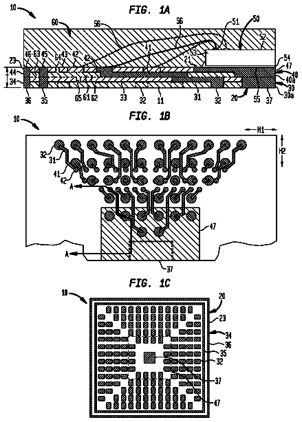
FIG. 1A is a diagrammatic top view of a stacked microelectronic unit according to an embodiment of the present invention.
FIG. 1B is a diagrammatic side sectional view of the microelectronic unit of FIG. 1A, taken along the line 1B-1B of FIG. 1A.
FIG. 1C is an enlarged diagrammatic side sectional view of a stage of fabrication of a chip connection portion of the microelectronic unit of FIG. 1A.
FIG. 1D is an enlarged diagrammatic side sectional view of a chip connection portion of the microelectronic unit of FIG. 1A.
FIG. 2A is a diagrammatic top view of a stage of fabrication of the microelectronic unit of FIG. 1A.
FIG. 2B is a diagrammatic side sectional view of the stage of fabrication of FIG. 2A, taken along the line 2B-2B of FIG. 2A.
FIG. 3A is a diagrammatic top view of a stage of fabrication of the microelectronic unit of FIG. 1A.
FIG. 3B is a diagrammatic side sectional view of the stage of fabrication of FIG. 3A, taken along the line 3B-3B of FIG. 3A.
FIG. 4 is a diagrammatic side sectional view of a stage of fabrication of the microelectronic unit of FIG. 1A.
FIG. 5A is a diagrammatic top view of a stage of fabrication of the microelectronic unit of FIG. 1A.
FIG. 5B is a diagrammatic side sectional view of the stage of fabrication of FIG. 5A, taken along the line 5B-5B of FIG. 5A.
FIG. 6 is a diagrammatic top view of a stage of fabrication of the microelectronic unit of FIG. 1A, showing a plurality of microelectronic units before they are diced into individual units.
FIG. 7 is a diagrammatic side sectional view of a stacked microelectronic unit according to another embodiment.
FIG. 8 is a diagrammatic side sectional view of a stacked microelectronic unit according to yet another embodiment.
FIG. 9 is a diagrammatic side sectional view of a microelectronic unit according to still another embodiment.
FIG. 10 is a diagrammatic side sectional view of a stacked microelectronic unit according to yet another embodiment.
FIG. 11A is a diagrammatic side sectional view of a stacked microelectronic unit according to another embodiment.
FIG. 11B is a diagrammatic side sectional view of the microelectronic unit of FIG. 11A, taken along the line 11B-11B of FIG. 11A.
FIG. 11C is a diagrammatic side sectional view of the microelectronic unit of FIG. 11A, taken along the line 11C-11C of FIG. 11A.
FIG. 11D is a stacked variation of the diagrammatic side sectional view shown in FIG. 11B.
FIG. 12 is a diagrammatic side sectional view of a stacked microelectronic assembly according to another embodiment.
FIG. 13 is a schematic depiction of a system according to one embodiment including a plurality of modules.
FIG. 14 is a diagrammatic side sectional view of a variation of the microelectronic unit of FIG. 1B.
Detailed description
With reference to FIGS. 1A and 1B, a microelectronic unit 10 according to an embodiment of the present invention can include a lead frame 20 having a plurality of monolithic lead fingers 25 extending in a plane P of the lead frame, each lead finger having a fan-out portion 30 and a chip connection portion 40. First and second device chips 50 and 60 can be electrically coupled to the lead frame 20. An encapsulant 70 can cover the device chips 50 and 60 and a portion of the lead fingers 25.
Examples of lead frame structures are shown and described in U.S. Pat. Nos. 7,176,506 and 6,765,287, the disclosures of which are hereby incorporated by reference herein. In general, a lead frame such as the lead frame 20 is a structure formed from a sheet of conductive metal, such as copper, that is patterned into segments including a plurality of lead fingers 25. The lead fingers 25 can then be used to form electrical connections to various other conductive structures for carrying an electronic signal potential to and from the device chips 50 and 60. In one example, the lead fingers 25 can be usable to carry an address signal usable to address a memory storage element in at least one of the first and device chips 50 and 60.
Each fan-out portion 30 extends in the lead frame plane P. The fan-out portions 30 have first and second opposed surfaces 31 and 32 and a first thickness T1 in a first direction between the opposed surfaces. Each fan-out portion 30 has a first width W1 in a second direction substantially parallel to the lead frame plane P. As used herein, "parallel" refers to axes extending through the structures' centroids being parallel or substantially parallel within an allowed tolerance, even if edges of the "parallel" structures are not entirely parallel. The fan-out portions 30 can include electrically conductive terminals (not shown) exposed at one or more of the first and second surface 31 and 32 for electrical interconnection with an external component such as a package substrate or a PCB.
In FIGS. 1A and 1B, the directions parallel to the first surface 31 are referred to herein as "horizontal" or "lateral" directions, whereas the directions perpendicular to the first surface are referred to herein as upward or downward directions and are also referred to herein as the "vertical" directions. The directions referred to herein are in the frame of reference of the structures referred to. Thus, these directions may lie at any orientation to the normal or gravitational frame of reference. A statement that one feature is disposed at a greater height "above a surface" than another feature means that the one feature is at a greater distance in the same orthogonal direction away from the surface than the other feature. Conversely, a statement that one feature is disposed at a lesser height "above a surface" than another feature means that the one feature is at a smaller distance in the same orthogonal direction away from the surface than the other feature.
Each chip connection portion 40 extends in the lead frame plane P from a corresponding fan-out portion 30. The chip connection portions 40 have a second thickness T2 in the first direction smaller than the first thickness T1. The chip connection portions 40 have a second width W2 in the second direction smaller than the first width W1. The chip connection portions 40 define a first recess 21 below the first surface 31 of the fan-out portions 30 and a second recess 22 below the second surface 32 of the fan-out portions.
The device chips 50 and 60 can each be a semiconductor chip, a wafer, or the like. For example, one or both of the first microelectronic element 20 and the second microelectronic element 30 can include a memory storage element such as a DRAM. As used herein, a "memory storage element" refers to a multiplicity of memory cells arranged in an array, together with circuitry usable to store and retrieve data therefrom, such as for transport of the data over an electrical interface.
Each of the device chips 50 and 60 can be a device chip having a plurality of at least one of passive devices or active devices. In one example, one or both of the device chips 50 and 60 can embody a plurality of active semiconductor devices therein. In another example, one or both of the device chips 50 and 60 can have a plurality of passive devices, the passive devices including at least one of capacitors, inductors, or resistors.
Each of the device chips 50 and 60 can include respective electrically conductive contacts 55 and 65 exposed at the respective front surfaces 51 and 61 thereof. As described herein, the electrically conductive contacts 55 and 65 of the first and second device chips 50 and 60 can also be referred to as "chip contacts." As used in this disclosure, a statement that an electrically conductive element is "exposed at" a surface of a structure indicates that the electrically conductive element is available for contact with a theoretical point moving in a direction perpendicular to the surface toward the surface from outside the structure. Thus, a terminal or other conductive element which is exposed at a surface of a structure can project from such surface; can be flush with such surface; or can be recessed relative to such surface and exposed through a hole or depression in the structure.
In a particular example, the first device chip 50 can overlie and can be electrically coupled with the second device chip 60 through electrical interconnections extending at least one of along or within the first and second device chips. In one embodiment, the first device chip 50 can entirely overlie the second chip 60. In an exemplary embodiment, at least one peripheral edge 53 of the first device chip 50 can be offset in the lead frame plane P from a corresponding peripheral edge 63 of the second device chip 60. In a variation of FIG. 1B, shown in FIG. 14, a microelectronic unit 1410 can have a second device chip 60 that can entirely overlie the first device chip 50.
As seen in FIGS. 1A and 1B, the first and second device chips 50 and 60 can be stacked relative to one another. In some embodiments, the front surface 51 of the first device chip 50 and the front surface 61 of the second device chip 60 can face one another. At least a portion of the front surface 51 of the first device chip 50 can overlie at least a portion of the front surface 61 of the second device chip 60. At least a portion of the second device chip 60 can project beyond a lateral edge 53 of the first device chip 50. Accordingly, the contacts 65 of the second device chip 60 can be positioned in a location projecting beyond the lateral edge 53 of the first device chip 50.
The contacts 55 and 65 of the first and second device chips 50 and 60 can be exposed at the front surfaces 51 and 61 adjacent respective peripheral edges 53 and 63. For example, the contacts 55 and 65 can be arranged in one or two parallel rows adjacent the peripheral edges 53 and 63 of the front surfaces 51 and 61.
In example embodiments, the first and second device chips 50 and 60 can be flip-chip bonded directly onto the chip connection portions 40 of the lead fingers 25, which can extend under the front surfaces 51 and 61 of the first and second device chips. In such an embodiment, the contacts 55 and 65 on the first and second device chips 50 and 60 can be electrically connected to the chip connection portions 40 through respective bumps 41 and 42 extending from the respective top surface 43 and bottom surface 44 of the chip connection portions. In an alternative embodiment, the bumps 41 and 42 can extend from the respective contacts 55 and 65 of the first and second device chips 50 and 60.
In one embodiment, the contacts 55 of the first device chip 50 can be joined with some of the chip connection portions 40a, and the contacts 65 of the second device chip 60 can be joined with some of the chip connection portions 40b. As shown in FIG. 1A, the chip connection portions 40a that are electrically connected with the first device chip 50 can be longer and extend farther from the inner edges 33 of the fan-out portions than the chip connection portions 40b that are electrically connected with the second device chip 60.
As shown in the side sectional view in FIG. 1B, some of the chip connection portions 40 can be joined with the contacts 55 and the contacts 65 of either one or both of the first and second device chips 50 and 60 through respective bumps 41 and 42. In one example, some of the chip connection portions 40 can be joined with contacts of both the first and second device chips 50 and 60 when the device chips include memory storage elements, e.g., volatile memory such as dynamic random access memory ("DRAM") or non-volatile memory such as flash memory, among others. In an exemplary embodiment, some of the chip connection portions 40 can be joined with contacts of both the first and second device chips 50 and 60, where such shared chip connection portions can be usable to carry power or a reference potential. In all of the embodiments disclosed herein, any of the chip connection portions can be joined with a first device chip at a top surface of the chip connection portion, a second device chip at a bottom surface of the chip connection portion, or both a first and second device chip at respective top and bottom surfaces of the chip connection portion.
In a particular embodiment, connections between the contacts 55 and 65 of the first and second device chips 50 and 60 and the chip connection portions 40a and 40b can be offset in a direction in the lead frame plane P in which the chip connection portions 40a and 40b extend towards the respective fan-out portions 30.
In one example, the microelectronic unit 10 can also include a passive component 12 electrically connected between at least a first one of the connection portions 40 and a second one of the connection portions. In one embodiment, such a passive component 12 can be a decoupling capacitor extending between connection portions 40, one or more of the connection portions being usable to carry power, and one or more of the connection portions being usable to carry a reference potential.
In a particular example, the bumps 41 and 42 can be in the form of metal pillars extending from the respective chip connection portions 40a and 40b. In one example, the bumps 41 and 42 can be gold stud bumps. In one embodiment, the bumps 41 and 42 can be in the form of a conductive matrix material extending between the connection portions 40 and the respective contacts 55 and 65 of the first and second device chips 50 and 60. In one example, a metal can be plated onto the bumps 41 and 42 for joining with the conductive contacts 55 and 65 of the device chips 50 and 60, the metal selected from the group consisting of: gold, nickel, palladium, tin, or an alloy of any of these metals.
In one embodiment, the bumps 41 and 42 can include conductive masses. Such conductive masses can comprise a fusible metal having a relatively low melting temperature, e.g., solder, tin, or a eutectic mixture including a plurality of metals. Alternatively, the conductive masses can include a wettable metal, e.g., copper or other noble metal or non-noble metal having a melting temperature higher than that of solder or another fusible metal. In a particular embodiment, the conductive masses can include a conductive material interspersed in a medium, e.g., a conductive paste, e.g., metal-filled paste, solder-filled paste or isotropic conductive adhesive or anisotropic conductive adhesive.
Each of the device chips 50 and 60 is shown disposed within a corresponding recess 21 or 22. In one embodiment, at least a portion of the thickness of each device chip 50 and 60 extends within a corresponding recess 21 or 22, such that the front surface 51 and 61 of each respective device chip is disposed below the respective first and second surfaces 31 and 32. As shown in FIG. 1B, the entire thickness of each device chip 50 and 60 extends within the corresponding recess 21 or 22, such that the rear surface 52 and 62 of each respective device chip is disposed below the respective first and second surfaces 31 and 32.
In one example, the first and second recesses 21 and can be defined between inner edges 33 of the fan-out portions 30, such that the fan-out portions are disposed beyond the exterior periphery 53 and 63 of the respective device chips 50 and 60.
The encapsulant 70 can cover the device chips 50 and 60 and the chip connection portions 40 of the lead fingers 25. The encapsulant 70 can cover, for example, the rear surfaces 52 and 62 of the first and second device chips 50 and 60. In a particular embodiment, the encapsulant 70 can be an overmold. A portion of the encapsulant 70 can extend between the first and second device chips, such that the encapsulant can cover the front surfaces 51 and 61 of the first and second device chips 50 and 60.
A method of fabricating the microelectronic unit 10 (FIGS. 1A and 1B) will now be described, with reference to the FIGS. 1C through 5B. As shown in FIGS. 2A and 2B, a metal layer 20a can be provided. Material can be removed from the first surface 31 of the metal layer 20a to form a central opening 21a extending from the first surface towards the second surface 32 of the metal layer.
While the central opening 21a is being formed, additional material can be removed from the metal layer 20a to form a plurality of monolithic lead fingers 25 extending in a plane of the metal element. Material can be removed from between adjacent ones of the lead fingers 25 to form peripheral openings 21b extending from the first surface 31 towards the second surface 32 of the metal layer.
The central opening 21a and the peripheral openings 21b can be formed for example, by selectively etching the metal layer 20a, after forming a mask layer where it is desired to preserve remaining portions of the metal layer. For example, a photoimageable layer, e.g., a photoresist layer, can be deposited and patterned to cover only portions of the first surface 31, after which a timed etch process can be conducted to form the central opening 21a and the peripheral openings 21b. In one example, the central opening 21a can extend to a distance 23a from the first surface 31 that is farther from the first surface than a distance 23b to which the peripheral openings 21b extend.
Then, referring to FIGS. 3A and 3B, material can be removed from the first surface 31 of the lead fingers 25 to expand portions of the peripheral openings 21b to become peripheral openings 21c, thereby defining the fan-out portions 30 and the connection portions 40a and 40b (collectively the connection portions 40) extending from the fan-out portions. A portion of the central opening 21a and the peripheral openings 21c together form the first recess 21 extending beneath the first surface 31 and between inner surfaces 33 of the fan-out portions 30. The peripheral openings 21c can be formed using the same processes described above with respect to FIGS. 2A and 2B. In one example, the central opening 21a can extend to a distance 23a from the first surface 31 that is farther from the first surface than a distance 23c to which the peripheral openings 21c extend.
Next, referring to FIG. 4, material can be removed from the second surface 32 of the metal layer 20a to complete the formation of the plurality of lead fingers 25. Material can be removed from between adjacent ones of the lead fingers 25 to deepen the peripheral openings 21c so that they extend completely through the metal layer 20a from the first surface 31 to the second surface 32. A portion of the central opening 21a and the deepened peripheral openings 21c together form the second recess 22 extending beneath the second surface 32 and between inner surfaces 33 of the fan-out portions 30. The peripheral openings 21c can be deepened using the same processes described above with respect to FIGS. 2A and 2B.
Next, referring to FIGS. 5A and 5B, contacts 55 of the first device chip 50 can be joined to bumps 41 extending from a top surface 43 of the connection portions 40a. In one example, the bumps 41 can be formed as shown in FIGS. 1C and 1D. As shown in FIG. 1C, an initial bump 41a can have a photoresist 45 overlying a top surface 46 thereof. An etch process can remove material of the initial bump 41a from the side surfaces 47 thereof between the top surface 46 and the top surface 43 of the connection portions 40a. As shown in FIG. 1D, when enough material is removed from the side surfaces 47, the portion of the initial bump 41a adjacent the top surface 46 can be removed, so that the bump 41 remains.
Subsequently, referring again to FIGS. 1A and 1B, contacts 65 of the second device chip 60 can be joined to bumps 42 extending from a bottom surface 44 of the connection portions 40b. In one example, a conductive matrix material can be applied to the bumps 41 and 42 or the bumps can be in the form of by a conductive matrix material extending between the connection portions 40 and the respective contacts 55 and 65 of the first and second device chips 50 and 60. In a subsequent sintering process, the lead frame 20 can be heated to a sintering temperature in which the conductive matrix material undergoes changes which then permanently electrically and mechanically joins the contacts 55 and 65 of the first and second device chips 50 and 60 to the connection portions 40.
As deposited, i.e., before sintering, the conductive matrix material can include particles or flakes of a high melting-point material such as copper or silver, and particles or flakes a low melting-point material, such as tin, bismuth, or a combination of tin and bismuth. Some particles may have a structure which includes metal or non-metal cores, for example, polymer, silica or graphite cores, and a different metal such as a low melting-point metal thereon.
In some examples, the conductive matrix material may include a "reactive" or uncured polymer. After deposition, the structure can be subsequently heated to a temperature for sintering the conductive matrix material. During this sintering process, the high and low melting point metals fuse together, typically forming intermetallics therebetween, and forming a solid matrix of metal which can have an open cell foam-like appearance. The deposited conductive matrix material may include a medium which escapes from the metallic component thereof during the sintering process, such as by evaporation, such that the conductive matrix material may have voids therein. Alternatively, the conductive matrix material may include a reactive polymer component. Typically, the polymer component cross-links and cures as a result of the sintering process. The polymer component can become interspersed throughout the metal matrix as a result of the sintering process, the polymer material typically being connected together in open cells of the metal matrix. The metal matrix and polymer interspersed throughout may then form a solid conductive structure.
Under certain conditions, after sintering, the conductive matrix material can form a solid structure which subsequently cannot be reflowed except at a temperature substantially higher than the temperature at which the sintering process is performed. Such result may be obtained by sintering particularly when a low melting-point metal, e.g., tin or bismuth, is substantially consumed in the formation of intermetallics with at least one other metal component, of the conductive material, e.g., copper.
The description continues in the full USPTO document.
 Lapsed, fee not paid18 drawings