Technical field
The present invention relates to a semiconductor light emitting element which emits light by combining an electron and hole(s) combining in a semiconductor, and an illuminating apparatus using the semiconductor light emitting element, and more particularly to a method for improving light extraction efficiency of a semiconductor light emitting element which has an emission peak in the shorter wavelength side from red light.
Background art
In a semiconductor light emitting element in which an n-type semiconductor layer, a light emitting layer and a p-type semiconductor layer are laminated on a growth substrate having optical transparency with the emission wavelength of the light emitting layer, a method for forming a reflection film having high reflectance on the side opposite to the surface, from which the light emitted from the light emitting layer is extracted, has been used as a means of improving light extraction efficiency (or external quantum efficiency). This is because the light generated in the semiconductor light emitting layer has a nature to be emitted in all directions, and as FIG. 8 shows, more lights are emitted diagonally (the output angle is large) than lights emitted upward from the emission point (the output angle is small), so most of the lights emitted from the light emitting layer are lost after performing multiple reflection inside the element.
FIG. 9 shows a change of light extraction efficiency with respect to the change of the reflectance of the reflection film. As FIG. 9 shows, 95% or higher reflectance is required to increase the light extraction efficiency to be 70% or higher, and in this 95% or higher area, light extraction efficiency improves about 6% if the reflectance improves only 1%. In the case of a GaAs semiconductor, high reflectance is implemented, and light extraction efficiency can be improved by using Au as a material of an electrode, which also functions as the reflection film.
However the reflectance of a metal greatly depends on the wavelength, and this method cannot be used on oxide or nitride compound semiconductor light emitting elements which have an emission peak in the shorter wavelength side from red light. For example, ohmic contact cannot be guaranteed between a GaN material and a high reflection metal, such as silver and aluminum. Therefore a laminated electrode of such a metal as Ni, Pt or Rh, such a metal oxide as ITO (Indium Tin Oxide), and a high reflection metal, is used, which makes it difficult to obtain a reflectance higher than the natural reflectance of the high reflection metal.
In Non-patent Document 1, a prior art to solve this problem is proposed. In this prior art, an SiO.sub.2 film with 1/4 optical wavelength is layered between silver as the high reflection metal and a pGaN layer, which is a semiconductor layer, in order to guarantee a reflectance higher than the natural reflectance of the high reflection metal, and higher reflectance is obtained for all the incident angles compared with the case of silver film alone. By this, an ODR (Omni-Directional Reflector) is formed and the average reflectance becomes 98% when calculated with a 450 nm wavelength. The ohmic contact is guaranteed by means of micro-contacts in which RuO.sub.2 (ruthenium oxide) film is formed between the above mentioned pGaN layer and the SiO.sub.2 film, and the silver layer is electrically connected with the pGaN layer via the RuO.sub.2 film through the openings formed in the SiO.sub.2 film.
This prior art is supposed to implement high reflectance for all the incident angles, but as a result of the present inventors performing similar calculations, it was found out, as shown in FIG. 10, that the reflectance drops about 20% in a wide angle range centered around 55.degree. if the film thickness of SiO.sub.2 film has a 1/8 optical wavelength film thickness (0.5Q), and the reflectance drops about 30% in an angle range centered around 45.degree. if the SiO.sub.2 film thickness has 1/4 optical wavelength film thickness (1Q). The probable reason is that if a single layer of SiO.sub.2 film is formed on metal as a reflection film, good reflection can be obtained at a 1/4 optical wavelength film thickness (1Q) when the incident angle is small, but as the incident angle increases, light which effuses from the semiconductor layer to the SiO.sub.2 film as shown by the broken line in FIG. 11, in other words, light called "near field wave" or "evanescent wave" couples with the silver film layer. In FIG. 10, 1/4 optical wavelength film thickness=.lamda./(4n)=1Q, n is a refractive index. In FIG. 10, in order to obtain the data characteristics written in Non-patent Document 1, that is 98% reflectance, using an average value of each reflectance at 0 to 90.degree. incident angle, the thickness of the reflection film must be increased to 5Q or 6Q.
As FIG. 12 shows, the above mentioned effusing amount is zero until the incident angle .theta. is critical angle .theta.c, and light effuses up to the depth of about wavelength .lamda. at critical angle .theta.c, then it exponentially decreases. .theta.c=30.degree. to 40.degree.. Non-patent Document 1: GaInN light-emitting diodes with RuO.sub.2, OSiO.sub.2, OAg omni-directional reflector (Jong Kyu Kim, Thomas Gesmann, Hong Luo and E. Fred Schubert, Applied Physics Letters, 84, 4508 (2004), Rensselaer Polytechnic Institute)
Disclosure of the invention
It is an object of the present invention to provide a semiconductor light emitting element which can improve the light extraction efficiency, and an illuminating apparatus using this element.
A semiconductor light emitting element or an illuminating apparatus according to an aspect of the present invention has an n-type semiconductor layer having optical transparency with an emission wavelength of a light emitting layer; the light emitting layer; and a p-type semiconductor layer, which are laminated; and a reflection film which is disposed on a side opposite to a surface from which light emitted from the light emitting layer is extracted, wherein the reflection film comprises: a transparent layer having optical transparency with the emission wavelength of the light emitting layer; and a metal layer, which is laminated on a side opposite to the light emitting layer and is constituted by a metal material having a high reflectance, and the transparent layer has a refractive index lower than the refractive index of a layer disposed on a side of the light emitting layer when viewed from the transparent layer, with the emission wavelength, and a thickness of the transparent layer is equal to or more than a value obtained by dividing a value of 3/4 of the emission wavelength by the refractive index of the transparent layer.
According to this configuration, in a semiconductor light emitting element in which at least an n-type semiconductor layer, a light emitting layer and a p-type semiconductor layer are laminated in this order, or in a reverse order on a substrate which has optical transparency with the emission wavelength of the light emitting layer, and has a conductive buffer layer on a conductive substrate or insulating substrate, so as to be conductive, or on a growth substrate such as an insulating substrate which is separated after the semiconductor layer is grown, a reflection film is disposed on the side opposite to the surface from which light, emitted from the light emitting layer, is extracted. The reflection film is comprised of a transparent layer that has a refractive index lower than the refractive index of the layer disposed at the light emitting layer side with the emission wavelength of the light emitting layer, and has a thickness which is equal to or more than a value obtained by dividing a value of 3/4 of the emission wavelength by the refractive index of the transparent layer, and a metal layer which is laminated on the transparent layer, and is constituted by a metal material having a high reflectance.
Therefore the light which entered at a relatively small angle (small incident angle) less than the critical angle .theta.c is reflected by the transparent layer or the metal layer. The light which entered at a relatively large angle (large incident angle) exceeding the critical angle .theta.c becomes the effusing light, called the "near field wave" or the "evanescent wave", which effuses from the interface between the growth substrate constituted by GaN having high refractive index, or the semiconductor layer, and the reflection film to the transparent layer at the interface. However if the transparent layer has a thickness obtained by dividing a value of 3/4 of the emission wavelength by the refractive index of the transparent layer, the possibility of the light passing through the transparent layer and being absorbed by the metal layer decreases, and most of the lights return from the transparent layer to the interface (reflected), and reenter the growth substrate or the semiconductor layer via the interface, and propagate toward the light extraction surface.
Therefore lights which entered the reflection film at all kinds of incident angles can be extracted efficiently, and less power consumption is needed to extract the same amount of light, and brightness can be increased with supplying the same amount of power.
Brief description of the drawings
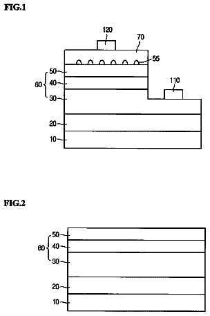
FIG. 1 is a cross-sectional view depicting the structure of a light emitting diode, which is a semiconductor light emitting element according to an embodiment of the present invention.
FIG. 2 is a cross-sectional view depicting the structure of a light emitting diode, which is a semiconductor light emitting element according to an embodiment of the present invention.
FIG. 3 is a cross-sectional view depicting the structure of a light emitting diode, which is a semiconductor light emitting element according to an embodiment of the present invention.
FIG. 4 a cross-sectional view depicting the structure of a light emitting diode, which is a semiconductor light emitting element according to an embodiment of the present invention.
FIG. 5 is a graph depicting a change of reflectance with respect to the thickness of the change of the transparent layer when silver is used for the metal layer in the metal layer and transparent layer constituting the reflection film in each of the light emitting diodes.
FIG. 6 is a graph depicting the changes of reflectance (R), transmittance (T) and absorptance (A) with respect to the change of film thickness of the silver reflection film.
FIG. 7 is a graph enlarging a partial area of FIG. 6.
FIG. 8 is a graph depicting the change of luminous flux with respect to each output direction from the light emitting layer.
FIG. 9 is a graph depicting the change of the light extraction efficiency with respect to the change of reflectance of the reflection film.
FIG. 10 is a graph depicting the actual change of reflectance with respect to the change of incident angle of the light to the reflection film according to a prior art.
FIG. 11 is a diagram depicting an evanescent wave (near field wave).
FIG. 12 is a graph depicting the change of the light effusing amount due to the evanescent wave with respect to the incident angle.
FIG. 13 is a graph depicting the relationship of the thickness of the transparent layer (SiO.sub.2) and the reflectance of the reflection film.
FIG. 14 are diagrams depicting the calculation conditions and the calculation method for the graph shown in FIG. 13.
FIG. 15 is a graph depicting the relationship of the thickness t of the metal layer and the weighted average reflectance <R> of the reflection film.
FIG. 16 are diagrams depicting the calculation conditions for the graph shown in FIG. 15.
FIG. 17 is a graph depicting the relationship of the thickness t of the Al layer when the metal layer is constructed by forming the Al layer between the Ag layer and the transparent layer, and the weighted average reflectance <R> of the reflection film.
FIG. 18 is a diagram depicting the calculation conditions for the graph shown in FIG. 17.
FIG. 19 are plan views depicting an example of the transparent layer shown in FIG. 1 or FIG. 2, where FIG. 19A shows the general view, and FIG. 19B shows an enlarged view of a part of the transparent layer.
FIG. 20 are plan views depicting another example of the transparent layer shown in FIG. 1 or FIG. 2, where FIG. 20A shows a general view, and FIG. 20B shows an enlarged view of a part of the transparent layer.
FIG. 21 is a graph depicting the relationship of the area occupying ratio of Pt, when the transparent conductive layer is formed to be mesh or island shapes with a 1 nm thickness using Pt, and forward voltage Vf of the light emitting diode, and the weighted average reflectance <R>.
FIG. 22 is a table showing the experiment result of examining the relationship of the thickness of the Pt layer and the degree of adhesion (tensile strength).
Best mode for carrying out the invention
FIG. 1 to FIG. 4 are cross-sectional views depicting configurations of the light emitting diodes 1 to 4, which are semiconductor light emitting elements according to an embodiment of the present invention. The configurations in FIG. 1 to FIG. 4 are typical configuration examples of the semiconductor light emitting elements to which the present invention is applied, and the light emitting diode 1 in FIG. 1 is a flip-chip type, and the light emitting diodes 2 to 4 in FIG. 2 to FIG. 4 are wire bonding types.
The light emitting diode 1 in FIG. 1 has an n-type semiconductor layer 11, a light emitting layer 12 and a p-type semiconductor layer 13, which are laminated, and has a reflection film which is disposed on the side opposite to a light extracting surface 14 from which light emitted from the light emitting layer 12 is extracted. Noteworthy here is that the p-type electrode is the reflection film A according to the present invention. The reflection film A has: a transparent layer 15 which has a refractive index lower than the refractive index of the p-type semiconductor layer 13 to which this reflection film contacts, and a thickness equal to or greater than the 3/4 optical wavelength (3Q) in an emission wavelength of the light emitting layer 12; and a metal layer 16 which is laminated on the transparent layer 15, and is made of a metal material having a high reflectance.
As mentioned later, metal portions 15b, which are in the form of a mesh or a plurality of islands through the transparent layer 15 to electrically connect the p-type semiconductor layer 13 and the metal layer 16 are disposed in a part of the transparent layer 15. As FIG. 1 shows, a transparent conductive layer 19 (first electrode layer) may be laminated between the p-type semiconductor layer 13 and the transparent layer 15.
Each of the above layers 11 to 13 is made of the III-V group semiconductor or the II-VI group semiconductor, and in the case of GaN, for example, has a wavelength .lamda. of about 455 nm and a refractive index of about 2.5. The transparent layer 15 is made of SiO.sub.2, for example, and has a refractive index of about 1.43. The metal layer 16 is made of silver, for example. After the layers are formed up to the metal layer 16, one corner thereof is removed, and the n-type electrode 17 connected to the n-type semiconductor layer 11 is formed. Further, after the growth substrate is stripped, the stripped surface is roughened to form the light extracting surface 14. The configuration shown in FIG. 1 is completed.
In the light emitting diode 2 in FIG. 2 as well, an n-type semiconductor layer 21, a light emitting layer 22 and a p-type semiconductor layer 23 are laminated on a growth substrate, which is not illustrated, and a reflection film is disposed on the surface opposite to a light extracting surface 24 for light emitted from the light emitting layer 22. Noteworthy here is that the p-type electrode is the reflection film B according to the present invention. The reflection film B is comprised of a transparent layer 25 having a refractive index lower than the refractive index of the p-type semiconductor layer 23 to which this reflection film B contacts, and a thickness equal to or greater than 3/4 optical wavelength (3Q) in an emission wavelength of the light emitting layer 22, and a metal layer 26 which is laminated on the transparent layer 25 and is made of a metal material having a high reflectance. Each of the layers 21 to 23 is made of a III-V group semiconductor or a II-VI group semiconductor, such as GaN, and the transparent layer 25 is made of SiO.sub.2, for example, and the metal layer 26 is made of silver, for example. After the layers are formed up to the metal layer 26, the growth substrate is stripped, the stripped surface is roughened to form the light extracting surface 24, and an n-type electrode 27 is formed on the roughened surface. Accordingly, the metal layer 26 serves as the p-type contact. The configuration shown in FIG. 2 is completed.
As mentioned later, metal portions 25b, which are in the form of a mesh or a plurality of islands through the transparent layer 25 to electrically connect the p-type semiconductor layer 23 and the metal layer 26, are disposed in a part of the transparent layer 25. As FIG. 2 shows, the transparent conductive layer 29 (first electrode layer) may be laminated between the p-type semiconductor layer 23 and the transparent layer 25.
In the light emitting diode 3 in FIG. 3, on the other hand, an interface 30a is roughened, and an n-type semiconductor layer 31, a light emitting layer 32 and a p-type semiconductor layer 33 are laminated on a growth substrate (or laminated substrate) 30 which is transparent in the emission wavelength of the light emitting layer 32, and a reflection film is disposed on a surface opposite to a light extracting surface 34 for light emitted from the light emitting layer 32. Noteworthy here is that the rear face of the growth substrate 30 bears the reflection film C according to the present invention. The reflection film C is comprised of a transparent layer 35 which has a refractive index lower than the refractive index of the growth substrate 30 to which this reflection film contacts, and a thickness equal to or greater than 3/4 optical wavelength (3Q) in the emission wavelength of the light emitting layer 32, and a metal layer 36 which is laminated on the transparent layer 35 and is made of a metal material having a high reflectance. The growth substrate 30 is made of GaN, ZnO and Al.sub.2O.sub.3. Each of the layers 31 to 33 is made of a III-V group semiconductor or II-VI group semiconductor, and in the case of GaN, for example, has a wavelength .lamda. of about 455 nm, and a refractive index of about 2.5. The transparent layer 35 is made of SiO.sub.2, for example, and has a refractive index of about 1.43. The metal layer 36 is made of silver, for example. After a transparent conductive layer 38 is formed on the p-type semiconductor layer 33, and the transparent layer 35 and the metal layer 36 are formed on the rear face side, and an n-type electrode 37 and a p-type electrode 39 are formed on a removed corner portion and the transparent conductive layer 38. Thus, the configuration shown in FIG. 3 is completed. The n-type semiconductor layer 31 and the p-type semiconductor layer 33 may be replaced. In this case, the electrode 37 serves as the p-type and the electrode 39 serves as the n-type.
In the light emitting diode 4 in FIG. 4, an n-type semiconductor layer 41, a light emitting layer 42 and a p-type semiconductor layer 43 are laminated on a transparent growth substrate (or laminated substrate) 40 transparent in the emission wavelength of the light emitting layer 42, and a reflection film is disposed on a face side opposite to a light extracting surface 44 for light emitted from the light emitting layer 42. The rear face side of the growth substrate 40 bears a reflection film D having a transparent layer 45 and a metal layer 46, similar to the above mentioned transparent layer 35 and the metal layer 36. The difference from FIG. 3 is that the top of the p-type semiconductor layer 43 which serves as the light extraction surface 44 is roughened. In the light emitting diode 4 as well, the n-type semiconductor layer 41 and the p-type semiconductor layer 43 may be replaced, and the n-type electrode 47 and the p-type electrode 49 may be the p-type and the n-type respectively.
In this way, according to the present embodiment, the reflectance is improved not by utilizing the 1/4 optical wavelength thin film interference as in the case of the above mentioned Non-patent Document 1, but by utilizing the total reflection effect when the light enters from a medium having a high refractive index (e.g. GaN material: refractive index=2.5) to a medium having a low refractive index (e.g. SiO.sub.2: refractive index=about 1.43). As the reflection film, the reflection layer is formed by the transparent layer 15, 25, 35 or 45 having a thickness equal to or greater than the 3/4 optical wavelength film thickness, and the metal layer 16, 26, 36 or 46 made of silver, silver alloy, Al or Al alloy and laminated on the transparent layer. The rough structure for making the mirror reflection angles irregular is formed in the light extracting surface 14, 24 or 44, or the interface 30a. Thereby a higher average reflectance can be seen to be obtained from the view of the actual radiation angle distribution of light from the light emitting layer 12, 22, 32 or 42 shown in FIG. 8, although it is difficult in the range of small incident angle .theta. to accomplish improvement of the reflectance to exceed those in the case of being laminated with laminating the 1/4 optical wavelength film according to Non-patent Document 1.
In concrete terms, in the interface between the growth substrate 30 or 40, or the semiconductor layer 13 or 23 having a high refractive index and the reflection film, the light having a relatively large incident angle exceeding the critical angle .theta.c is likely to diffuse from the interface to the transparent layer 15, 25, 35 or 45, as the so-called "near field waves" or "evanescent waves". However, since the transparent layer 15, 25, 35 or 45 has a thickness equal to or greater than the 3/4 optical wavelength, there is little possibility that the light passes through the transparent layer 15, 25, 35 or 45 and is then absorbed by the metal layer 16, 26, 36 or 46, but there is high possibility that the light returns from the transparent layer 15, 25, 35 or 45 to the interface (i.e., reflected), and enter the growth substrate 30 or 40 or the semiconductor layer 13 or 23 again from the interface, and propagate to the light extracting surface 14, 24, 34 or 44.
The light which has not been extracted by one transmission and reflected back to the inside in this way has a statistical distribution similar to the initial emission, because the angle transforming function is performed depending on the incident angle, refractive index and shape at the roughened surface of the light extracting surface 14, 24 or 44 or the interface 30a. Therefore, from the view of the weighted average reflectance for all the incident angles that is obtained based on the radiation angle distribution, higher reflectance can be seen to be obtained compared with the case of laminating the 1/4 optical wavelength film according to Non-patent Document 1. In this way, light which has entered the reflection film at any incident angle can be extracted efficiently, and less power consumption is needed to extract the same amount of light, and brightness can be increased by supplying the same amount of power. In this film configuration, precise film thickness control is unnecessary and a lower number of film layers are required, thereby making the processing easier.
In FIG. 1 to FIG. 4, the minutely roughened structures are exemplary shown as a configuration of making the mirror reflection angle to be disturbed, however, the present invention is not limited to this structure. The purpose should be noted to eliminate the multiple reflection of repeating the mirror reflection in a rectangular parallelepiped. A slope may be created on the side face of the element by changing the macro structure of the element, or the element itself may have a truncated pyramid shape.
FIG. 5 shows the change of reflectance with respect to the change of thickness of the transparent layer 15, 25, 35 or 45, when silver is used for the metal layer 16, 26, 36 or 46. The abscissa denotes a film thickness N, and this film thickness N is indicated by a multiple n of the 1/4 optical wavelength (1Q). As the above mentioned FIG. 11 and FIG. 12 show, the film thickness of the transparent layer 15, 25, 35 or 45, which utilizes the total reflection effect, must be one optical wavelength or more. FIG. 5 shows the above mentioned weighted average reflectance considering the radiant flux distribution shown in FIG. 8. Accordingly, it will be seen from FIG. 5 that the transparent layer 15, 25, 35 or 45 is enough to have a thickness of 3/4 optical wavelength or more because having a reflectance of 99% or more.
The transparent layer 15 or 25 (later mentioned transparent portion 15c or 25c) and the transparent layer 35 or 45 are not limited to the above mentioned SiO.sub.2, but may be ZrO.sub.2 or may be Al.sub.2O.sub.3 or the like, having a refractive index between the refractive indexes 1.43 and 1.95 of SiO.sub.2 and ZrO.sub.2 respectively. If the light emitting semiconductor element is made of II-VI group ZnO material, however, SiO.sub.2 is preferable for the transparent layer 15, 25, 35 or 45 to utilize the total reflection effect, since the refractive index of ZnO is about 2.0 (the refractive index difference is small and the total reflection effect is weak if Al.sub.2O.sub.3 or ZrO.sub.2 is used). In FIG. 5, the reflectance characteristic of ZrO.sub.2 is also shown.
For the transparent layer 15 or 25 (later mentioned transparent portions 15c or 25c) and the transparent layer 35 or 45, SiO.sub.2, ZrO.sub.2, Al.sub.2O.sub.3, TiO.sub.2, Ta.sub.2O.sub.5, MgF, CaF or Si.sub.3N.sub.4, for example, can be used. These transparent layers or transparent portions may be constructed as a multilayer structure, in which a plurality of layers are laminated. Each layer laminated in this way may be made of a material selected from the above mentioned materials, or layers made of different materials may be laminated.
The total reflection effect can be obtained only if the thickness of the transparent layer 15, 25, 35 or 45 is the 3/4 optical wavelength or more, as mentioned above. However the film actually deposited has film stress, and this film stress increases as the thickness of the film increases, and the films separate during processing or during use of the element, although this depends on the film deposition method. Therefore if the thickness of the transparent layer 15, 25, 35 or 45 is 5/4 optical wavelength or less, both the optical characteristic and the film stability can be implemented. When the transparent layer 15, 25, 35 or 45 is laminated, the film stress can be easily weakened by using sputtering, but the semiconductor layer is damaged in some cases, therefore if EB (Electron Beam) deposition, which causes less damage is used instead, the film stress can be easily increased, as mentioned above.
FIG. 13 is a graph depicting the relationship of the thickness of the transparent layer 15, 25, 35 or 45 (SiO.sub.2), and the reflectance of the reflection film A, B, C or D. In FIG. 13, the weighted average reflectance <R> in the ordinate is a reflectance considering the solid angle distribution. FIG. 14A and FIG. 14B are diagrams depicting the conditions to calculate the weighted average reflectance <R> in FIG. 13. FIG. 14C is a diagram depicting the method for calculating the weighted average reflectance <R> considering the solid angle distribution.
In FIG. 14A and FIG. 14B, the refractive index n of the transparent layer (SiO.sub.2) is 1.43, the reflective index n of the semiconductor layer (GaN) is 2.4, and the wavelength .lamda. of the light is 450 nm. Then in FIG. 13, the optical wavelength film thickness Q becomes Q=450/(4.times.1.43)=78.7 nm. The weighted average reflectance <R> is a reflectance of the interface of the transparent layer (SiO.sub.2).
In FIG. 14C, the term of sin .phi., in the right hand side of expression of the weighted average reflectance <R>, is multiplied and convolution-integrated, whereby weighting according to the incident angle of the light is performed.
According to FIG. 13, if the thickness t of the transparent layer (SiO.sub.2) is 3Q (a value obtained by dividing a value of 3/4 of the emission wavelength by the refractive index of the transparent layer) or more, the weighted average reflectance <R> becomes 96% or more, and the weighted average reflectance <R> no longer increases even if the thickness t increases more, for both cases of using Ag for the metal or using Al for the metal layer. Therefore it is preferable that the thickness t of the transparent layer 15, 25, 35 or 45 is 3Q or more.
If the thickness t of the transparent layer (SiO.sub.2) is 5Q (a value obtained by dividing a value of 5/4 of the emission wavelength by the refractive index of the transparent layer) or more, the weighted average reflectance <R> becomes approximately constant, so the reflectance improvement effect can no longer be implemented even if the thickness t is increased. Therefore it is preferable that the thickness t of the transparent layer 15, 25, 35 or 45 is 3Q to 5Q.
If the metal layer 16, 26, 36 or 46 is made of silver or a silver alloy, and is laminated with the transparent layer 15, 25, 35 or 45, the reflectance average 98% to 99% or more can be obtained, as shown in FIG. 5, and high light extraction efficiency can be implemented. The high reflection metal, however, is not limited to silver material, but Al is desirable for the light emitting element in the ultraviolet region. In the case of laminating the transparent layer 15, 25, 35 or 45 on Al as well, the average reflectance can be higher than the reflectance of Al alone, since the radiant flux is small in the incident angle area in which the reflectance of Al contributes, and the total reflection effect contributes in the area where the incident angle is large.
FIG. 6 shows the film thickness and reflectance (R), transmittance (T) and absorptance (A) when the refractive index (n, k) of silver is (0.066, 2.5), although the values change depending on the film deposition method and film deposition conditions. Therefore in order to implement high reflectance, it is preferable that the film thickness is 80 nm or more, with which 90% or higher reflectance can be obtained. However it is preferable that the film thickness is 200 nm or less, since separation due to film stress easily occurs if the film thickness increases. It is especially preferable that the film thickness is about 100 nm in terms of implementing both reflectance and film stability.
For the metal layer 16, 26, 36 or 46, Al or an Al alloy, for example, can be used instead of silver or silver alloy.
FIG. 15 is a graph depicting the relationship of the thickness t of the metal layer 16, 26, 36 or 46 (Ag or Al) and the weighted average reflectance <R> of the reflection film A, B, C or D. FIG. 16A and FIG. 16B are diagrams depicting the conditions to calculate the weighted average reflectance <R> in FIG. 15.
According to FIG. 15, if Ag is used for the metal layer, the graph becomes approximately flat when the thickness t of the metal layer is 80 nm or more, and the weighted average reflectance <R> does not increase even if the thickness t is increased more. If Al is used for the metal layer, the graph becomes approximately flat when the thickness t of the metal layer is 50 nm or more, and the weighted average reflectance <R> does not increase even if the thickness t is increased more.
Therefore if Ag is used for the metal layer, the thickness t of the metal layer is preferably 80 nm or more, but about 80 nm is more preferable, since a reflectance close to the maximum can be obtained with a minimum thickness.
If Al is used for the metal layer, the thickness t of the metal layer is preferably 50 nm or more, but about 50 nm is more preferable, since a reflectance close to the maximum can be obtained with the minimum thickness.
The metal layer 16, 26, 36 or 46 may be constructed as a multilayer structure in which a plurality of layers are laminated. Each layer laminated in this way may be made of a material selected from the above mentioned materials, or layers made of different materials may be laminated.
If the metal layer 16, 26, 36 or 46 is constituted by Ag or an Ag alloy, degree of adhesion with the transparent layer 15, 25, 35 or 45 (SiO.sub.2) is low, and therefore the metal layer 16, 26, 36 or 46 and the transparent layer 15, 25, 35 or 45 may easily separate. Degree of adhesion of Al and an Al alloy to the transparent layer 15, 25, 35 or 45 is higher than that of Ag and an Ag alloy. Therefore if an Al or Al alloy layer is formed and an Ag or Ag alloy layer is formed thereon, so that the Al or the Al alloy layer is inserted between the transparent layer 15, 25, 35 or 45 (SiO.sub.2) and the Ag or Ag alloy layer, then the metal layer 16, 26, 36 or 46 and the transparent layer 15, 25, 35 or 45 do not easily separate.
FIG. 17 is a graph depicting the relationship of the thickness t of the Al layer in the case of forming the metal layer by inserting the Al layer between the Ag layer and the transparent layer, and the weighted average reflectance <R> of the reflection film A, B, C or D. FIG. 18 is a diagram depicting the conditions to calculate the weighted average reflectance <R> in FIG. 17.
According to FIG. 17, when the thickness t of the Al layer is 1 nm, the weighted average reflectance <R> is 99.0%, that is, an extremely good weighted average reflectance <R> is obtained. Therefore it is preferable that the thickness t of the Al layer is 1 nm or less. If the thickness t of the Al layer is 3 nm, the weighted average reflectance <R> is 98.3%, which is equivalent to the reflectance of aluminum in the bulk. Since the light reflectance of Al is lower than Ag, if the thickness t of the Al layer becomes 3 nm or more, the reflectance becomes the same as the case of constructing the metal layer only with an Al layer, without using the Ag layer. Hence the thickness t of the Al layer must be thinner than 3 nm.
In the light emitting diodes 3 and 4 in FIG. 3 and FIG. 4, the transparent layer 35 or 45 and the metal layer 36 or 46 are formed on the growth substrate 30 or 40, which is a portion not related to the path of the diode current, but in the light emitting diodes 1 and 2 in FIG. 1 and FIG. 2, the metal layer 16 or 26 becomes the p-type electrode, and the transparent layer 15 or 25 is formed on the p-type semiconductor layer 13 or 23, that is, formed on the path of the diode current. If the reflection film A or B is formed on the p-type semiconductor layer 13 or 23 and plays the role of the p-type electrode as well, as in this case, the transparent conductive layer 19 or 29 is laminated between the p-type semiconductor layer 13 or 23 and the transparent layer 15 or 25, as shown in FIG. 1 and FIG. 2.
The transparent conductive layer 19 or 29 has conductivity (has ohmic contact) with the p-type semiconductor layer 13 or 23, and is a first electrode layer which is transparent with the emission wavelength of the light emitting layer 12 or 22. The transparent layer 15 or 25 having openings (via holes) 15a or 25a is formed on the transparent conductive layer 19 or 29. If the metal layer 16 or 26 is laminated on the transparent layer 15 or 25, the metal material of the metal layer 16 or 26 is laminated on the transparent layer 15 or 25 via the openings 15a or 25a, and the metal portions 15b or 25b is formed by the metal material laminated inside the openings 15a or 25a.
By these metal portions 15b or 25b, the transparent conductive layer 19 or 29 and the metal layer 16 or 26 are electrically conducted. Thereby the metal layer 16 or 26 is electrically conducted with the p-type semiconductor layer 13 or 23 via the metal portions 15b or 25b and the transparent conductive layer 19 or 29, and is used as the p-type electrode (second electrode layer).
If the Pt layer of which thickness 0.1 nm to 0.3 nm is formed between the transparent conductive layer 19 or 29 (e.g. ITO) and the metal portions 15b or 25b (e.g. Ag), degree of adhesion between the transparent conductive layer 19 or 29 (e.g. ITO) and the metal portions 15b or 25b (e.g. Ag), can be further improved.
In this way, when the reflection film plays a role of the electrode and ohmic contact is required, the openings 15a or 25a are formed by forming micro contact holes in the transparent layer 15 or 25 which utilizes the total reflection effect, or by dividing the area of the transparent layer 15 or 25 to be a mesh, and these openings 15a or 25a are covered with the metal layer 16 or 26 having a high reflectance, whereby the metal portions 15b or 25b are formed. As a result, ohmic contact between the metal layer 16 or 26 and the transparent conductive layer 19 or 29 becomes possible. Because of this configuration, the semiconductor layer 13 or 23 and the metal layer 16 or 26 having high reflectance can be electrically connected without sacrificing an increase of the reflectance by the transparent layer 15 or 25, and sufficient current can be injected into the light emitting layer 12 or 22.
FIG. 19 and FIG. 20 are plan views depicting examples of the transparent layer 15 or 25 shown in FIG. 1 or FIG. 2. FIG. 19A and FIG. 20A show general views respectively, and FIG. 19B and FIG. 20B show enlarged views of a part of the transparent layer respectively.
In the transparent layer 15 or 25 shown in FIG. 19A, a plurality of transparent portions 15c or 25c, having a hexagonal island shape, for example, are disposed. The metal portions 15b or 25b are formed in a mesh so as to fill the spaces between each transparent portion 15c or 25c. The shape of the transparent portion 15c or 25c is not limited to a hexagon, but may be a circle, for example, or other shapes.
In the transparent layer 15 or 25 shown in FIG. 20A, a plurality of metal portions 15b or 25b having a circular island shape, for example, are disposed. The transparent portions 15c or 25c are formed in a mesh so as to fill the spaces between each metal portion 15b or 25b. The shape of the transparent portion 15c or 25c is not limited to a hexagon, but may be a circle, for example, or other shapes.
In the transparent layer 15 or 25, current does not flow through the transparent portions 15c or 25c. Therefore the current for having an LED emit reaches the transparent conductive layer 19 or 29 from the metal layer 16 or 26, which is a p-type electrode, via each metal portion 15b or 25b, then flows from the transparent conductive layer 19 or 29 to the p-type semiconductive layer 13 or 23, light emitting layer 12 or 22, and n-type semiconductor layer 11, and the light emitting layer 12 or 22 emits light.
In order for the light emitting layer 12 or 22 to uniformly emits lights at this time, the current which reached the transparent conductive layer 19 or 29 must flow under the transparent portions 15c or 25c (space between the transparent portions 15c or 25c and the p-type semiconductor layer 13 or 23). As the size of the transparent portion 15c or 25c is smaller, the current can more easily flow under the transparent portions 15c or 25c.
The description continues in the full USPTO document.
 Lapsed, fee not paid6 drawings