 Lapsed, fee not paid16 drawings
Vehicles & Drones · US 11,235,757 B2
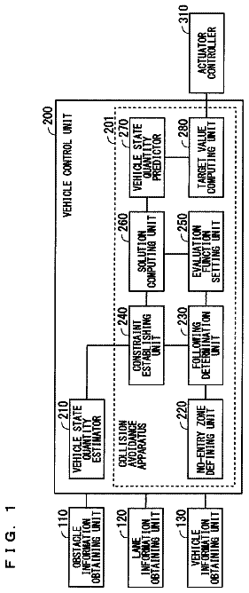
Collision avoidance apparatus
Provided is a collision avoidance apparatus that can avoid a collision through both steering and braking.
US 11,235,780 B2 · Assignee: HITACHI AUTOMOTIVE SYSTEMS, LTD. · Inventors: Shinoda; Hiroshi et al.
Sheet 1 of 12 from the published document. All sheets in the USPTO PDF
A transient increase/decrease of power supplied to a reconfiguration circuit to be a logic circuit whose circuit configuration can be changed is reduced. An autonomous traveling control ECU has a reconfiguration circuit, a function control unit, a power supply circuit, and a power supply control unit. The reconfiguration circuit is a reconfigurable logic circuit. The function control unit determines an operation mode of the reconfiguration circuit on the basis of a mode determination signal and controls a reconfiguration of the reconfiguration circuit on the basis of a determination result. The power supply circuit supplies power to the reconfiguration circuit. The power supply control unit controls the power supply circuit. The power supply control unit 206 controls a load current generated by the power supply circuit before a load variation of the reconfiguration circuit, on the basis of power supply control information to be information for controlling the power supply circuit.
An automatic operation is a system that can solve various social problems including reducing the number of accidents and resolving congestion and efforts towards commercialization thereof become active every year worldwide. In the automatic operation system, it is necessary to detect a vehicle, a pedestrian, a white line, and the like from a sensor input of a camera, a radar, and the like and transmit them to a driver or control a brake and a steering. Therefore, simultaneous processing of advanced recognition algorithms or a plurality of algorithms is required. In order to respond to this demand, improving the performance of the automatic operation system by using a field-programmable gate array (FPGA) in addition to a CPU is under examination. The FPGA is a reconfiguration circuit capable of changing a logic circuit and has a feature that processing provided in a plurality of pieces of
1 of 12 drawing sheets so far from the published document, cropped to the drawing. Every sheet is in the USPTO PDF.
What the patent claimed, word for word. All of it is now free to use.
The present invention relates to an electronic control device, an in-vehicle system, and a power supply control method and particularly, to technology effective for controlling a power supply that supplies power to a logic circuit whose circuit configuration can be changed.
An automatic operation is a system that can solve various social problems including reducing the number of accidents and resolving congestion and efforts towards commercialization thereof become active every year worldwide. In the automatic operation system, it is necessary to detect a vehicle, a pedestrian, a white line, and the like from a sensor input of a camera, a radar, and the like and transmit them to a driver or control a brake and a steering. Therefore, simultaneous processing of advanced recognition algorithms or a plurality of algorithms is required.
In order to respond to this demand, improving the performance of the automatic operation system by using a field-programmable gate array (FPGA) in addition to a CPU is under examination.
The FPGA is a reconfiguration circuit capable of changing a logic circuit and has a feature that processing provided in a plurality of pieces of hardware can be performed on one circuit. Of course, the present invention is not limited to the above logic circuit and a whole electronic circuit is used only when power is supplied from a power supply circuit.
Meanwhile, in an electronic apparatus such as a portable computer, by adopting a power management scheme in a predetermined operation mode and appropriately switching a function of a selected assembly in the electronic apparatus to invalidity or validity, consumption is reduced.
If the function of the assembly of the electronic apparatus is validated or invalidated, a load of the electronic apparatus changes, an output voltage from a power supply device transiently decreases and increases, and a data error, an automatic reset, or the like can be caused.
As technology for reducing the transient voltage variation, for example, there is technology for determining a load state of at least one circuit block as a function of an enable signal or a clock signal and causing the power supply device to control the output current with the output current of the power supply device as a function of the load state of at least one circuit block (for example, refer to PTL 1).
Further, as technology for smoothing an output voltage of the power supply circuit, technology for providing an output capacitor between an output terminal of the power supply and a ground terminal is widely known. CITATION LIST Patent Literature
PTL 1: JP 2004-336986 A SUMMARY OF INVENTION Technical Problem
In the automatic operation system, it is necessary to respond instantaneously to unexpected situations such as jumping of the pedestrian. Therefore, it is necessary to execute reconfiguration processing of the logic circuit in a short time. When the reconfiguration processing transits to algorithm processing, a load current of the logic circuit greatly increases in a short time. In contrast, when the algorithm processing transits to the reconfiguration processing, the load current of the logic circuit greatly decreases in a short time.
In the power supply circuit with the FPGA as the load, the output voltage transiently decreases and increases according to the rapid increase and decrease in the load current described above.
In this case, if the output voltage of the power supply circuit is out of an allowable range of the FPGA, there is a problem in that the possibility of causing the data error or the automatic reset increases. Therefore, the power supply circuit that supplies a current to the FPGA is required to have a function of supplying a constant voltage at all times even if the rapid load variation occurs.
However, in the technology disclosed in PTL 1, in order to control the circuit block, that is, to estimate the load state of the circuit block from the enable signal or the clock signal to change the load state of the circuit block, the control of the power supply circuit should be performed after the load variation. As a result, it is considered that it is difficult to sufficiently suppress the transient voltage variation.
With respect to the output capacitor to be used for smoothing the output voltage of the power supply circuit, if the load increase of the logic circuit becomes more rapid, a capacitor having a larger capacity is required and it is apprehended that a cost or an mounting area increases.
An object of the present invention is to provide technology capable of reducing a transient increase/decrease in power supplied to a logic circuit whose circuit configuration can be changed.
The above and other objects and novel features of the present invention will become apparent from the description of the present specification and the accompanying drawings. Solution to Problem
An outline of a representative invention of the inventions disclosed in the present application is simply described as follows.
That is, a representative electronic control device has a reconfiguration circuit, a function control unit, a power supply circuit, and a power supply control unit. The reconfiguration circuit is a reconfigurable logic circuit. The function control unit determines an operation mode of the reconfiguration circuit on the basis of a mode determination signal showing an operation mode of a vehicle and controls a reconfiguration of the reconfiguration circuit on the basis of a determination result. The power supply circuit supplies a power supply voltage to the reconfiguration circuit. The power supply control unit controls the power supply circuit.
The power supply control unit controls a supply current generated by the power supply circuit before a load variation of the reconfiguration circuit, on the basis of power supply control information to be information for controlling the power supply circuit.
Particularly, power supply control information has the operation mode of the reconfiguration circuit and control information in the power supply circuit corresponding to the operation mode. Further, the power supply control unit acquires the control information corresponding to the operation mode determined by the function control unit from the power supply control information.
Furthermore, the electronic control device has a power supply control database storing the power supply control information. The power supply control unit searches for the control information corresponding to the operation mode determined by the function control unit from the power supply control information stored in the power supply control database. Advantageous Effects of Invention
Effects obtained by a representative invention of the inventions disclosed in the present application are simply described as follows.
A transient increase/decrease of an output voltage of a power supply circuit that supplies power to a reconfiguration circuit to be a logic circuit whose circuit configuration can be changed can be reduced.
By the above (1), an electronic control device with high reliability can be realized.
FIG. 1 is a block diagram showing an example of a configuration of an in-vehicle system according to a first embodiment.
FIG. 2 is a block diagram showing an example of a configuration of an autonomous traveling control ECU included in the in-vehicle system of FIG. 1 .
FIG. 3 is an explanatory diagram of a mode database included in an autonomous traveling control logic unit of FIG. 2 .
FIG. 4 is an explanatory diagram of a processing item database included in the autonomous traveling control logic unit of FIG. 2 .
FIG. 5 is an explanatory diagram of a power supply control database included in the autonomous traveling control logic unit of FIG. 2 .
FIG. 6 is a flowchart showing an example of power supply control processing in a power supply control unit of FIG. 2 .
FIG. 7 is a sequence diagram showing an example of power supply control processing in the power supply control unit of FIG. 2 .
FIG. 8 is a sequence diagram showing an example of operation mode extension in the in-vehicle system of FIG. 1 .
FIG. 9 is a block diagram showing another example of the autonomous traveling control ECU of FIG. 2 .
FIG. 10 is an explanatory diagram showing an example of a configuration of an autonomous traveling control ECU according to a second embodiment.
FIG. 11 is a schematic diagram of an inductor current waveform and an output voltage change to show an effect of power supply control by a power supply control unit of FIG. 10 .
FIG. 12 is an explanatory diagram of a power supply control database included in the autonomous traveling control ECU of FIG. 10 .
FIG. 13 is an explanatory diagram showing another configuration example of the autonomous traveling control ECU of FIG. 10 .
In the following embodiments, the invention will be described in a plurality of sections or embodiments when required as a matter of convenience. However, these sections or embodiments are not irrelevant to each other unless otherwise stated and one relates to the entire or part of the other as a modification, details, or a supplementary explanation thereof.
Further, in the following embodiments, when referring to the number of elements (including the number of pieces, numerical values, amounts, ranges, and the like), the number of the elements is not limited to a specific number unless otherwise stated or except for the case in which the number is apparently limited to a specific number in principle and the number larger or smaller than the specified number is also applicable.
Furthermore, in the following embodiments, it goes without saying that components (including element steps and the like) are not always indispensable unless otherwise stated or except for the case in which the components are apparently indispensable in principle.
Similarly, in the following embodiments, when shapes of the components, a positional relation thereof, and the like are mentioned, the substantially approximate and similar shapes and the like are included therein unless otherwise stated or except for the case in which it is conceivable that they are not apparently excluded in principle. The same is applicable to the numerical values and the ranges described above.
Further, in all the drawings for explaining the embodiments, the same reference numerals are attached in principle to the same members and the repetitive description thereof is omitted. Even in a plan view, hatching may be added to facilitate understanding of the drawings.
Hereinafter, the embodiments will be described in detail. First Embodiment
<Outline>
In an in-vehicle system 10 according to a first embodiment, an autonomous traveling control ECU 201 has a reconfiguration circuit 209 that is a reconfigurable logic circuit, a function control unit 207 that controls a reconfiguration of the reconfiguration circuit 209 , a power supply circuit 211 that supplies a power supply voltage to the reconfiguration circuit 209 , and a power supply control unit 206 that controls the power supply circuit 211 .
Further, the autonomous traveling control ECU 201 has a power supply control database 212 in which power supply control information corresponding to each operation ID to be a plurality of pieces of processing to the reconfiguration circuit 209 from the function control unit 207 or rewriting between the plurality of pieces of processing is stored.
The power supply control unit 206 extracts the power supply control information from the power supply control database 212 , on the basis of the operation ID received from the function control unit 207 . Further, the power supply control unit 206 controls the power supply circuit 211 supplying a power supply voltage to the reconfiguration circuit 209 , on the basis of the extracted power supply control information.
The embodiments of the present invention will be described in detail below on the basis of the drawings.
<Configuration Example of in-Vehicle System>
FIG. 1 is a block diagram showing an example of a configuration of an in-vehicle system according to the first embodiment.
The in-vehicle system 10 is, for example, a system for controlling autonomous traveling of a vehicle. As shown in FIG. 1 , the in-vehicle system 10 includes a camera 101 , a radar 102 , an own vehicle position sensor 103 , an automatic operation button 104 , a wireless communication device 105 , an auxiliary control ECU 106 , a brake control ECU (Electronic Control Unit: Electronic Control Device) 107 , an engine control ECU 108 , a power steering control ECU 109 , and an autonomous traveling control ECU 201 .
The camera 101 , the radar 102 , and the own vehicle position sensor 103 are external recognition sensors that recognize an external situation of the vehicle. The camera 101 and the radar 102 are sensors for recognizing the outside or obtaining a distance to a target object.
The own vehicle position sensor 103 is a sensor for detecting an own vehicle position by a global positioning system (GPS) or the like. The automatic operation button 104 is a button for starting automatic operation control or changing an automatic operation mode.
The wireless communication device 105 that is a communication device is connected to a wireless network not shown in the drawings for updating the in-vehicle system by OTA (Over-The-Air).
The autonomous traveling control ECU 201 that is an electronic control device is an automatic operation vehicle traveling control device. The auxiliary control ECU 106 is an auxiliary automatic operation vehicle traveling control device. The brake control ECU 107 is a control device that performs brake control of the vehicle, that is, braking force control.
The engine control ECU 108 is a control device that controls an engine generating a driving force of the vehicle. The power steering control ECU 109 is a control device that controls power steering of the vehicle.
Each of the camera 101 , the radar 102 , the own vehicle position sensor 103 , the automatic operation button 104 , and the wireless communication device 105 is connected to the autonomous traveling control ECU 201 . Update information including sensor information from the camera 101 , the radar 102 , and the own vehicle position sensor 103 , an automatic operation control signal from the automatic operation button 104 , and autonomous traveling control processing information from the wireless communication device 105 is transmitted to the autonomous traveling control ECU 201 .
Further, the autonomous traveling control ECU 201 , the auxiliary control ECU 106 , the brake control ECU 107 , the engine control ECU 108 , and the power steering control ECU 109 are connected so as to be able to communicate with each other by a controller area network (CAN), for example.
Here, when the autonomous traveling control ECU 201 receives a request to start the automatic operation by the automatic operation button 104 , the autonomous traveling control ECU 201 calculates a movement route of the vehicle on the basis of external information of the camera 101 , the radar 102 , the own vehicle position sensor 103 , and the like.
The autonomous traveling control ECU 201 outputs control commands such as braking and driving force to the brake control ECU 107 , the engine control ECU 108 , and the power steering control ECU 109 so as to move the vehicle according to the above route.
The brake control ECU 107 , the engine control ECU 108 , and the power steering control ECU 109 receive control commands for autonomous traveling control from the autonomous traveling control ECU 201 and output operation signals to each control target such as an actuator, for example.
That is, the autonomous traveling control ECU 201 is a main control device for outputting a control command and the brake control ECU 107 , the engine control ECU 108 , and the power steering control ECU 109 are sub-control devices for controlling the control target according to the control command from the autonomous traveling control ECU 201 .
The auxiliary control ECU 106 is an auxiliary control device for performing automatic operation control in place of the autonomous traveling control ECU 201 , when the autonomous traveling control ECU 201 is abnormal.
<With Respect to Autonomous Traveling Control ECU>
FIG. 2 is a block diagram showing an example of a configuration of the autonomous traveling control ECU 201 included in the in-vehicle system 10 of FIG. 1 .
The autonomous traveling control ECU 201 includes an autonomous traveling control logic unit 210 and a power supply circuit 211 . Here, it is assumed that the power supply circuit 211 supplies power to the reconfiguration circuit 209 . Further, in the autonomous traveling control logic unit 210 , it is assumed that power is supplied to each functional block other than the reconfiguration circuit 209 by a power supply circuit not shown in the drawings.
The autonomous traveling control logic unit 210 has communication interfaces 204 and 208 (hereinafter, described as the “communication interface 204 ” in the case of collectively designating the communication interfaces), an information collection unit 205 , a power supply control unit 206 , a function control unit 207 , a reconfiguration circuit 209 , a mode database 202 , a processing item database 203 , and a power supply control database 212 . Further, the function control unit 207 holds a circuit database (not shown in the drawings) to be described later.
The communication interface 204 is an interface performing communication according to a predetermined protocol, such as the CAN used in the in-vehicle system. The autonomous traveling control ECU 201 is connected to other device via the communication interface 204 and transmits and receives data.
In the present embodiment, the autonomous traveling control ECU 201 is connected to the camera 101 , the radar 102 , the own vehicle position sensor 103 , the automatic operation button 104 , and the wireless communication device 105 via the communication interface 204 .
Further, the autonomous traveling control ECU 201 is connected to the auxiliary control ECU 106 , the brake control ECU 107 , the engine control ECU 108 , and the power steering control ECU 109 via the communication interface 208 .
The information collection unit 205 collects sensor information from the camera 101 , the radar 102 , and the own vehicle position sensor 103 input from the communication interface 204 and an automatic operation control signal from the automatic operation button 104 and periodically transfers the collected sensor information and automatic operation control signal to the function control unit 207 .
If the information collection unit 205 receives update information including autonomous traveling control processing information, circuit data to be updated, and power supply control data from the wireless communication device 105 , the information collection unit 205 stores the circuit data to be updated in a circuit database not shown in the drawings and updates contents of the mode database 202 , the processing item database 203 , and the power supply control database 212 . Here, the wireless communication device 105 may be configured to be provided in the autonomous traveling control ECU 201 , for example.
The information collection unit 205 is connected to each database included in the autonomous traveling control logic unit 210 via a control line not shown in the drawings. An processing example of the update information will be described later using FIG. 8 .
On the basis of a mode determination signal such as the sensor information and the automatic operation control signal acquired from the information collection unit 205 , the function control unit 207 refers to the mode database 202 and first determines an operation mode such as an expressway entrance mode, an automatic parking mode, or an ECU abnormality mode.
Then, processing information showing how to execute necessary operation processing in the operation mode by the reconfiguration circuit 209 is determined. Specifically, the processing information means the number of divisions of a circuit region of the reconfiguration circuit 209 , circuit data for updating each circuit region, an operation time, and the like. The details of the mode database 202 and the processing item database will be described using FIGS. 3 and 4 to be described later.
Further, the function control unit 207 changes the reconfiguration circuit 209 on the basis of the processing information described above and causes the reconfiguration circuit 209 to execute processing of the corresponding operation mode. Here, a dotted line arrow between the function control unit 207 and the reconfiguration circuit 209 shows that the function control unit 207 transfers circuit data for reconfiguring a circuit from a circuit database not shown in the drawings and a completion notification thereof. Further, a solid line arrow between the function control unit 207 and the reconfiguration circuit 209 shows that an execution instruction or execution data of processing and an execution result thereof are transferred.
Furthermore, the function control unit 207 outputs a control command such as braking and driving force via the communication interface 208 , on the basis of a result of the processing executed by the reconfiguration circuit 209 .
The reconfiguration circuit 209 is a circuit for executing predetermined processing on data and is constituted by hardware capable of changing a circuit configuration such as the FPGA, for example. The circuit configuration of the reconfiguration circuit 209 is changed by the function control unit 207 according to the processing information described above and the reconfiguration circuit 209 executes predetermined processing.
The power supply control unit 206 acquires mode information and an internal timer value managed by the function control unit 207 from the function control unit 207 . Here, the internal timer value is a value of a counter incremented by an internal clock.
The power supply control unit 206 performs synchronization by updating the internal timer value of the power supply control unit 206 , on the basis of the acquired internal timer value. In the power supply control database 212 , information on a schedule of power supply control such as a control signal and timing to the power supply circuit 211 is stored.
The power supply control unit 206 performs power supply control so as to increase or decrease the current supplied by the power supply circuit 211 , on the basis of the power supply control database 212 and the internal timer value.
The details of the power supply control database 212 will be described later using FIG. 3 . Further, the details of the power supply control processing will be described later using FIGS. 4 and 5 . Here, the power supply circuit 211 has been described as a dedicated power supply circuit of the reconfiguration circuit 209 . However, the power supply circuit 211 may be a power supply circuit that supplies power to the entire autonomous traveling control logic unit 210 .
The respective function units of the autonomous traveling control logic unit 210 , that is, the information collection unit 205 , the function control unit 207 , and the power supply control unit 206 are constituted by a program executed by the autonomous traveling control logic unit 210 or a logic circuit for performing a predetermined operation, for example, the FPGA. For the sake of functional safety of the automatic operation, each function unit of the autonomous traveling control logic unit 210 may be constituted by a processor having a plurality of cores adopting a lock step system.
Further, the autonomous traveling control logic unit 210 may be physically configured on one electronic control device or may be logically or physically configured on a plurality of electronic control devices. The program of each function unit described above may operate on a separate thread on the same electronic control device or may operate on a virtual electronic control device constructed on resources of a plurality of electronic control devices.
<Various Databases>
FIG. 3 is an explanatory diagram of the mode database 202 included in the autonomous traveling control logic unit 210 of FIG. 2 .
The mode database 202 is referred to by the function control unit 207 of FIG. 2 and is obtained by associating information acquired from the information collection unit 205 with an operation mode to be selected. The mode database 202 has a mode selection condition 301 for selecting an operation mode on the basis of the information acquired from the information collection unit 205 and an operation mode 302 selected by the mode selection condition 301 .
For example, as an example of an application to the automatic operation, in the mode selection condition 301 , the case where the expressway entrance has been determined on the basis of the parameter information of the external recognition sensors such as the camera 101 , the radar 102 , and the own vehicle position sensor 103 shown in FIG. 1 may be set as a first mode selection condition and in the operation mode 302 , a first operation mode may be determined as a mode 1 .
Further, in the mode selection condition 301 , the case of receiving a control signal for automatic parking by the automatic operation button 104 of FIG. 1 may be set as a second mode selection condition and in the operation mode 302 , a second operation mode may be determined as a mode 2 .
Similarly, in the mode selection condition 301 , the case of detecting abnormality of the ECU as failure detection information may be set as a third mode selection condition and in the operation mode 302 , a third operation mode may be determined as a mode 3 .
FIG. 4 is an explanatory diagram of the processing item database 203 included in the autonomous traveling control logic unit 210 of FIG. 2 .
The processing item database 203 is referred to by the function control unit 207 of FIG. 2 and associates the operation mode 302 with processing contents of the corresponding mode. The processing item database 203 is obtained by associating a processing method 402 and processing information 1 ( 403 - 1 ) to processing information 3 ( 403 - 3 ) (in the case of collectively designating the processing information, they are described as the “processing information 403 ”) for each operation mode 401 .
The processing method 402 is obtained by designating order of one or more processing to be executed, a reconfiguration procedure of a circuit, and the like. The processing information 403 is processing information designated by the processing method 402 .
For example, when the operation mode 401 is the mode 1 , providing one circuit region on the reconfiguration circuit 209 of FIG. 2 and sequentially executing processing of the processing information 1 ( 403 - 1 ), processing of the processing information 2 ( 403 - 2 ), and processing of the processing information 3 ( 403 - 3 ) are held as the processing method 402 . In addition, circuit data A 1 for executing first processing of the mode 1 and a processing time T 11 thereof may be held as the processing information 1 ( 403 - 1 ).
Similarly, circuit data A 2 for executing second processing of the mode 1 and a processing time T 12 thereof may be held as the processing information 2 ( 403 - 2 ) and circuit data A 3 for executing third processing of the mode 1 and a processing time T 13 thereof may be held as the processing information 3 ( 403 - 3 ).
As an example of an application to the automatic operation, the first processing of the mode 1 may be set as sensing processing, the second processing of the mode 1 may be set as behavior prediction processing of a vehicle or a pedestrian, and the third processing of the mode 1 may be set as movement route calculation processing of the vehicle.
Further, when the operation mode 401 is the mode 2 , dividing the circuit region into two parts, sequentially executing processing of the processing information 1 ( 403 - 1 ) and the processing information 2 ( 403 - 2 ) in one region, and executing processing of the processing information 3 ( 403 - 3 ) in the other region may be held as the processing method 402 .
Similarly to when the operation mode 401 is the mode 1 , circuit data B 1 to B 3 for executing the first to third processing of the mode 2 , respectively, and processing times T 21 to T 23 thereof may be held as the processing information 403 .
As an example of an application to the automatic operation, any one of the first to third processing of the mode 2 may be set as empty parking space search processing. Further, when the operation mode 401 is the mode 3 , dividing the circuit region into three parts, executing respective processing of the processing information 1 ( 403 - 1 ), the processing information 2 ( 403 - 2 ), and the processing information 3 ( 403 - 3 ) in parallel may be held as the processing method 402 .
Similarly to when the operation mode 401 is the mode 1 , circuit data C 1 to C 3 for executing the first to third processing of the mode 3 , respectively, and processing times T 31 to T 33 thereof may be held as the processing information 403 .
As an example of an application to the automatic operation, any one of the first to third processing of the mode 3 may be set as trajectory securing processing to stop safely. Here, the example in which three pieces of information (processing information 1 ( 403 - 1 ) to processing information 3 ( 403 - 3 )) are held as the processing information 403 has been shown. However, four or more pieces of information may be held.
FIG. 5 is an explanatory diagram of the power supply control database 212 included in the autonomous traveling control logic unit 210 of FIG. 2 .
In the power supply control database 212 , information on a schedule of power supply control such as a control signal and timing to the power supply circuit 211 is stored.
The details will be described below. The power supply control database 212 is referred to by the power supply control unit 206 of FIG. 2 and associates an operation mode 501 and control information 0 ( 503 - 0 ) to control information 6 ( 503 - 6 ) (in the case of collectively designating the power supply control information, they are described as “power supply control information 503 ”) to be power supply control contents of the operation mode 501 .
For example, when the operation mode 501 is the mode 1 , a timer value TA 0 , a load current value IA 0 , and a processing time PA 0 may be held as the control information 0 ( 503 - 0 ). The timer value TA 0 is a timer value that considers timing to start writing a connection circuit to an interface with the function control unit 207 of FIG. 2 to the reconfiguration circuit 209 . The load current value IA 0 is a load current value of the reconfiguration circuit 209 during writing.
Similarly, a timer value TA 1 considering timing to start writing the circuit data A 1 for executing the first processing of the mode 1 to the reconfiguration circuit 209 , a load current value IA 1 of the reconfiguration circuit 209 during writing, and a processing time PA 1 may be held as the control information 1 ( 503 - 1 ).
As the control information 2 ( 503 - 2 ), a timer value TA 2 considering timing to start executing the first processing of the mode 1 , a load current value IA 2 of the reconfiguration circuit 209 during executing of the first processing, and a processing time PA 2 may be held.
As the control information 3 ( 503 - 3 ), a timer value TA 3 considering timing to start writing the circuit data A 2 for executing the second processing of the mode 1 to the reconfiguration circuit 209 , a load current value IA 3 of the reconfiguration circuit 209 during writing, and a processing time PA 3 may be held.
As the control information 4 ( 503 - 4 ), a timer value TA 4 considering timing to start executing the second processing of the mode 1 , a load current value IA 4 of the reconfiguration circuit 209 during executing of the second processing, and a processing time PA 4 may be held.
As the control information 5 ( 503 - 5 ), a timer value TA 5 considering timing to start writing the circuit data A 3 for executing the third processing of the mode 1 to the reconfiguration circuit 209 , a load current value IA 5 of the reconfiguration circuit 209 during writing, and a processing time PA 5 may be held.
As the control information 6 ( 503 - 6 ), a timer value TA 6 considering timing to start executing the third processing of the mode 1 , a load current value IA 6 of the reconfiguration circuit 209 during executing of the third processing, and a processing time PA 6 may be held.
Each load current value may hold a temporal average value of a load current, for example. Here, as described above, it is assumed that the power supply circuit 211 of FIG. 2 supplies power to only the reconfiguration circuit 209 . However, the power supply circuit 211 may be configured to supply power to the entire autonomous traveling control logic unit 210 . In this case, a load current value of the entire autonomous traveling control logic unit 210 is stored in the power supply control database 212 .
Further, the timer value is a value of a counter incremented by an internal clock, for example, is managed by the function control unit 207 of FIG. 2 , and is used for synchronization with the power supply control unit 206 . The timer value is adjusted so that the supply current of the power supply circuit 211 increases or decreases before the load current of the reconfiguration circuit 209 varies, in consideration of a signal delay between the function control unit 207 and the power supply control unit 206 or a control delay until the supply current of the power supply circuit 211 increases or decreases from starting of the power supply control processing by the power supply control unit 206 .
Before operating as the in-vehicle system, the power supply control database 212 may store each numerical value on the basis of an actual measurement value or a simulation value, or the power supply control unit 206 may create it on the basis of each information of the processing item database 203 acquired from the function control unit 207 and store it. Further, the power supply control information 503 may include a voltage value, a current value, or a control code for controlling the supply current of the power supply circuit 211 .
<Power Supply Control Processing>
Next, power supply control processing of the power supply control unit 206 will be described using FIGS. 6 and 7 .
FIG. 6 is a flowchart showing an example of power supply control processing in the power supply control unit 206 of FIG. 2 .
Here, an example in which the power supply control database 212 is previously created and stored and the power supply control unit 206 manages processing order by using an internal control ID is shown.
The internal control ID indicates each of numbers of the control information 0 to 6 of the power supply control information 503 in FIG. 5 . Further, description is given on the assumption that each of the function control unit 207 and the power supply control unit 206 of FIG. 2 includes an internal timer.
First, when the power supply control unit 206 starts power supply control processing (step S 600 ), before a reconfiguration circuit operation starts, the power supply control unit 206 acquires a mode information and a timer value from the function control unit 207 and updates an internal timer value of the power supply control unit 206 (step S 601 ).
After the processing of step S 601 , the power supply control unit 206 determines whether or not a value of an operation mode is the same as a previous mode value (step S 602 ). In the processing of step S 602 , when it is determined that the value of the operation mode is different from the previous mode value (NO), the power supply control unit 206 sets the internal control ID to 0 (step S 603 ).
On the other hand, when it is determined that the value of the operation mode is the same as the previous mode value (YES), the power supply control unit 206 sets the internal control ID to 1 (step S 604 ). This is to determine whether or not processing for writing the connection circuit to the interface with the function control unit 207 to the reconfiguration circuit 209 is necessary according to whether or not the operation mode is different from the previous mode. Of course, ID information of the connection circuit may be obtained from the function control unit 207 and it may be determined whether or not the ID information is the same as previous ID information.
After the processing of step S 603 or the processing of step S 604 , the power supply control unit 206 refers to the power supply control database 212 and maintains a waiting state until the timer value shown by the internal control ID and the internal timer value of the power supply control unit 206 are matched (Step S 605 ).
When it is determined by the processing of step S 605 that the timer values are matched (YES), a load current value and a processing time shown by the internal control ID are transmitted as a power supply control instruction to the power supply circuit 211 (step S 606 ). The power supply circuit 211 supplies a reference current value until the power supply circuit 211 receives the power supply control instruction. If the power supply circuit 211 receives the power supply control instruction, the power supply circuit 211 increases or decreases the supply current to become the load current value shown by the internal control ID and when the processing time shown by the internal control ID ends, the power supply circuit 211 supplies the reference current value again.
The reference current value may be set by considering a leak current when a supply target is only the reconfiguration circuit 209 . In the case of supplying power to the entire autonomous traveling control logic unit 210 , the reference current value may be set by considering a load current other than the reconfiguration circuit 209 .
Then, the power supply control unit 206 determines whether or not there is next processing (step S 607 ). The power supply control unit 206 can determine whether or not there is the next processing, from the power supply control database 212 of FIG. 5 .
When it is determined in step S 607 that there is the next processing (YES), the power supply control unit 206 increments an internal processing ID (step S 608 ) and returns to the processing of step S 605 to prepare for next processing.
When it is determined by the processing of step S 607 that there is not the next processing (NO), the power supply control unit 206 ends the power supply control processing (step S 609 ).
FIG. 7 is a sequence diagram showing an example of the power supply control processing in the power supply control unit 206 of FIG. 2 .
In FIG. 7 , the case where the operation mode 501 of the power supply control database 212 described in FIG. 5 is the mode 1 will be described as an example.
Here, it is assumed that the power supply control database 212 is previously created and stored.
First, the function control unit 207 acquires the mode information from the mode database 202 and checks whether or not the mode is switched. Furthermore, the internal timer value managed by the function control unit 207 is acquired (step S 700 ). Here, an example in which the mode is switched is shown.
Next, the function control unit 207 sends the mode information and the timer value to the power supply control unit 206 (step S 701 ). The power supply control unit 206 updates the internal timer value of the power supply control unit 206 on the basis of the timer value (step S 702 ).
The description continues in the full USPTO document.
About 6,809 words. The USPTO PDF has it with every drawing.
Fees are due 3.5, 7.5 and 11.5 years after grant. This patent expired on February 1, 2026, so the fee marked "not paid" was the one that went unpaid.
ELECTRONIC CONTROL DEVICE, IN-VEHICLE SYSTEM, AND POWER SUPPLY CONTROL METHOD
Filed Sep 2017 · published Oct 2019Electronic control device, in-vehicle system, and power supply control method
Filed Sep 2017 · granted Feb 2022Earlier publications, parents and continuations. None of them can still be enforced, or this patent would not be listed.
Prior art cited by the examiner or applicant. Useful when you check your own idea for novelty.
Everything on this page comes from the documents linked above.