Lapsed, fee not paid8 drawings
Hardware & Electronics · US 11,222,910 B2
High-speed image sensor
A backside-illuminated multi-collection-gate image sensor is expected to achieve ultra-high-speed imaging.
US 11,223,119 B2 · Assignee: AAC Technologies Pte. Ltd. · Inventors: Mai; Jianchun
Sheet 1 of 4 from the published document. All sheets in the USPTO PDF
A millimeter wave LTCC filter includes system ground layers, metallized vias, first and second probes, two adjacent ones of the system ground layers define one closed resonant cavity, each closed resonant cavity is provided with a plurality of metallized vias, and the metallized vias of different closed resonant cavities face right to each other, to form concentric hole structures; an aperture of each first metallized via is equal to an aperture of each fourth metallized via, and is smaller than an aperture of each second metallized via that is equal to an aperture of each third metallized via; one end of the first probe is inserted into the first closed resonant cavity and electrically connected with the first system ground layer, and the second probe is coaxially arranged with the first probe, and is inserted into the fourth closed resonant cavity and electrically connected with the second system ground layer.
The fifth generation mobile phone mobile communication standard is also known as the fifth generation mobile communication technology (5G). Future 5G networks are developing towards a direction of network diversification, broadband, integration and intelligence. With the popularization of various smart terminals, mobile data traffic explodes. With the gradual landing of 5G networks, the mobile phone communication band increases significantly. The millimeter wave full-frequency band of the 5G communication includes 26.5˜29.5 GHz and a relative bandwidth of 10.7%, and corresponding related millimeter wave radio frequency systems require good rejection performance out of a band of DC˜60 GHz. The millimeter wave filter made by the LTCC process has higher integration, a smaller device dimension and a lower loss, but has strict requirements for processing of a metallized via. Therefore, it is
1 of 4 drawing sheets so far from the published document, cropped to the drawing. Every sheet is in the USPTO PDF.
What the patent claimed, word for word. All of it is now free to use.
The present invention relates to an antenna, and more particularly, to a millimeter wave LTCC filter used in the field of communication electronic products.
The fifth generation mobile phone mobile communication standard is also known as the fifth generation mobile communication technology (5G). Future 5G networks are developing towards a direction of network diversification, broadband, integration and intelligence. With the popularization of various smart terminals, mobile data traffic explodes. With the gradual landing of 5G networks, the mobile phone communication band increases significantly.
The millimeter wave full-frequency band of the 5G communication includes 26.5˜29.5 GHz and a relative bandwidth of 10.7%, and corresponding related millimeter wave radio frequency systems require good rejection performance out of a band of DC˜60 GHz. The millimeter wave filter made by the LTCC process has higher integration, a smaller device dimension and a lower loss, but has strict requirements for processing of a metallized via.
Therefore, it is necessary to provide a new millimeter wave LTCC filter to solve the above problems.
Many aspects of the exemplary embodiment can be better understood with reference to the following drawings. The components in the drawings are not necessarily drawn to scale, the emphasis instead being placed upon clearly illustrating the principles of the present invention. Moreover, in the drawings, like reference numerals designate corresponding parts throughout the several views.
FIG. 1 is a perspective structural schematic diagram of a millimeter wave LTCC filter of the present invention;
FIG. 2 is a partial perspective structural schematic diagram of a millimeter wave LTCC filter of the present invention;
FIG. 3 is a structural schematic diagram of respective system ground layers of a millimeter wave LTCC filter of the present invention; and
FIG. 4 illustrates an S characteristic parameter curve of a millimeter wave LTCC filter of the present invention.
The present invention will be further illustrated with reference to the accompanying drawings and the embodiments.
Referring to FIGS. 1-3 , an embodiment of the present invention provides a millimeter wave LTCC filter 100 . The millimeter wave LTCC filter 100 includes system ground layers 1 , metallized vias 2 , a first probe 3 , and a second probe 4 .
The system ground layers 1 include, sequentially stacked from top to bottom at intervals, a first system ground layer 1 a , a second system ground layer 1 b , a third system ground layer 1 c , a fourth system ground layer 1 d , and a fifth system ground layer 1 e . In this embodiment, peripheral dimensions of the first system ground layer 1 a , the second system ground layer 1 b , the third system ground layer 1 c , the fourth system ground layer 1 d , and the fifth system ground layer 1 e are the same, and for example, they are all rectangles of the same size.
In this embodiment, the millimeter wave LTCC filter further includes a substrate layer sandwiched between two adjacent ones of the system ground layers, and the substrate layer is made of an LTCC material.
Two adjacent layers of the system ground layers 1 define one closed resonant cavity 5 . Five layers of the system ground layers 1 sequentially define, from top to bottom, a first closed resonant cavity 5 a , a second closed resonant cavity 5 b , a third closed resonant cavity 5 c , and a fourth closed resonant cavity 5 d , which have the same peripheral dimension.
The metallized vias 2 include, in a stacking direction of the system ground layers 1 , a plurality of first metallized vias 21 penetrating the first closed resonant cavity 5 a , a plurality of second metallized vias 22 penetrating the second closed resonant cavity 5 b , a plurality of third metallized vias 23 penetrating the third closed resonant cavity 5 c , and a plurality of fourth metallized vias 24 penetrating the fourth closed resonant cavity 5 d . The plurality of first metallized vias 21 , the plurality of second metallized vias 22 , the plurality of third metallized vias 23 , and the plurality of fourth metallized vias 24 are arranged right facing to one another. That is, the metallized vias 2 of the respective closed resonant cavities 5 are concentric hole structures.
In an embodiment, an aperture of the first metallized via 21 is equal to an aperture of the fourth metallized via 24 , an aperture of the second metallized via 22 is equal to an aperture of the third metallized via 23 , and the aperture of the first metallized via 21 is smaller than the aperture of the second metallized via 22 . The provision of the above structure adjusts sizes of the apertures of the metallized vias of the different closed resonant cavities 5 and changes equivalent dimensions of the respective closed resonant cavities 5 , that is, the metallized vias 2 of the same closed resonant cavity 5 having the same intervals are changed smaller, the equivalent dimensions of the closed resonant cavities are increased, and a self-resonant mode of the closed resonant cavities is changed, thereby achieving a larger bandwidth.
Specifically, a center-to-center distance between two adjacent ones of the first metallized vias 21 is smaller than 2 to 2.5 times the aperture of each of the first metallized vias 21 ; a center-to-center distance of two adjacent ones of the second metallized vias 22 is smaller than 2 to 2.5 times the aperture of each of the second metallized vias 22 ; a center-to-center distance of two adjacent ones of the third metallized vias 23 is smaller than 2 to 2.5 times the aperture of each of the third metallized vias 23 ; and a center-to-center distance of two adjacent ones of the fourth metallized vias 24 is smaller than 2 to 2.5 times the aperture of each of the fourth metallized vias 24 .
The first metallized vias 21 and the first closed resonant cavity 5 a form a first substrate integrated waveguide unit 10 . The second metallized vias 22 and the second closed resonant cavity 5 b form a second substrate integrated waveguide unit 20 . The third metallized vias 23 and the third closed resonant cavity 5 c form a third substrate integrated waveguide unit 30 . The fourth metallized vias 24 and the fourth closed resonant cavity 5 d form a fourth substrate integrated waveguide unit 40 .
In an embodiment, the first closed resonant cavity 5 a is of a rectangular structure, and the plurality of first metallized vias 21 are equally spaced along a circumference of the first closed resonant cavity 5 a , to define, for example, a rectangular structure.
The second closed resonant cavity 5 b is of a rectangular structure, and the plurality of second metallized vias 22 are equally spaced along a circumference of the second closed resonant cavity 5 b , to define, for example, a rectangular structure.
The third closed resonant cavity 5 c is of a rectangular structure, and the plurality of third metallized vias 23 are equally spaced along a circumference of the third closed resonant cavity 5 c , to define, for example, a rectangular structure.
The fourth closed resonant cavity 5 d is of a rectangular structure, and the plurality of fourth metallized vias 24 are equally spaced along a circumference of the fourth closed resonant cavity 5 d , to define, for example, a rectangular structure.
In combination with FIG. 3 , in an embodiment, two opposite ends of the second system ground layer 1 b are respectively provided with two second rectangular through holes 11 that penetrate therethrough and are arranged symmetrically. The two second rectangular through holes 11 are located in a region defined by the second metallized vias 22 .
Two opposite ends of the third system ground layer 1 c are respectively provided with two third rectangular through holes 12 that penetrate therethrough and are arranged symmetrically. The two third rectangular through holes 12 are located in a region defined by the third metallized vias 23 , and the second rectangular through holes 11 and the third rectangular through holes 12 are staggered.
The fourth system ground layer 1 d has the same structure as the second system ground layer 1 b and is provided with two fourth rectangular through holes 13 which are symmetrical. The two fourth rectangular through holes 13 are disposed right facing the two second rectangular through holes 11 .
The first closed resonant cavity 5 a communicates with the second closed resonant cavity 5 b through the second rectangular through holes 11 . The second closed resonant cavity 5 b communicates with the third closed resonant cavity 5 c through the third rectangular through holes 12 . The third closed resonant cavity 5 c communicates with the fourth closed resonant cavity 5 d through the fourth rectangular through holes 13 .
In an embodiment, the two second rectangular through holes 11 are respectively located on two opposite sides of a short axis of the second system ground layer 1 b , and the second rectangular through holes 11 extend along a short axis direction of the second system ground layer 1 b ; the two third rectangular through holes 12 are respectively located on two opposite sides of a long axis of the third system ground layer 1 c , and the third rectangular through holes 12 extend along a long axis direction of the third system ground layer 1 c.
One end of the first probe 3 is inserted into the first closed resonant cavity 5 a to form a feed structure.
The second probe 4 is arranged symmetrically with the first probe 3 , and one end of the second probe 4 is inserted into the fourth closed resonant cavity 5 d to form a feed structure. The above structure can be excited by the first probe 3 and the second probe 4 cooperating with a coaxial line respectively, and achieve a greater bandwidth, a smaller loss, and an easier interconnection with ceramic packaged microstrip antennas, thereby allowing an insertion loss of the millimeter wave LTCC filter of the present invention to be reduced from 1.8 dB to 1 dB compared to the structure in the related art.
In another embodiment, the first probe 3 is inserted into the first closed resonant cavity 5 a from a geometric center of the first closed resonant cavity 5 a and reaches the second system ground layer 1 b in the first closed resonant cavity 5 a , and specifically, it is inserted from a geometric center of the first system ground layer 1 a ; and the second probe 4 is inserted into the fourth closed resonant cavity 5 d from a geometric center of the fourth closed resonant cavity 5 d and reaches the fourth system ground layer 1 d in the fourth closed resonant cavity 5 d , and specifically, it is inserted from a geometric center of the fifth system ground layer 1 e.
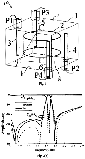
In combination with FIG. 4 , S 11 is a port reflection coefficient of the millimeter wave LTCC filter of the present invention, and S 21 is a transmission coefficient. The millimeter wave LTCC filter of the present invention has excellent performance, e.g., the insertion loss is smaller than 1 dB (S 21 is larger than −1 dB), and most of the out-of-band rejection is smaller than −30 dB, which meets requirements of the RF front end of the 5G millimeter wave communication system.
Compared with the related art, it is configured in the millimeter wave LTCC filter of the present invention that the respective closed resonant cavities have equal dimensions and the apertures of the metallized vias provided in the respective closed resonant cavities are adjusted in such a manner that equivalent dimensions of the respective closed resonant cavities are changed, the metallized vias having the same intervals are changed smaller, increase the equivalent dimensions of the closed resonant cavity are increased and a self-resonant mode of the closed resonant cavities is changed, thereby achieving a larger bandwidth and a smaller loss, which meets the requirements of the RF front end of the 5G millimeter wave communication system.
The above are only embodiments of the present invention and are not intended to limit the present invention. Any equivalent structures or equivalent flow variations, or direct or indirect applications in other related technical fields made by using the description and accompanying drawings of the present invention shall fall within the protection scope of the present invention.
About 2,111 words. The USPTO PDF has it with every drawing.
Fees are due 3.5, 7.5 and 11.5 years after grant. This patent expired on January 11, 2026, so the fee marked "not paid" was the one that went unpaid.
MILLIMETER WAVE LTCC FILTER
Filed Dec 2019 · published Jul 2020Millimeter wave LTCC filter
Filed Dec 2019 · granted Jan 2022Earlier publications, parents and continuations. None of them can still be enforced, or this patent would not be listed.
Prior art cited by the examiner or applicant. Useful when you check your own idea for novelty.
Everything on this page comes from the documents linked above.